GPS module time display unit
Source: InternetPublisher:92IFHY1t0 Keywords: GPS module time display Updated: 2025/12/05
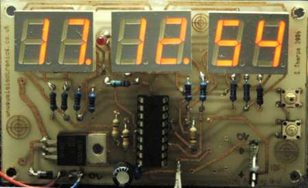
I decided to build a device to permanently display the accurate time received by an inexpensive GPS module installed in my studio. I acquired a PIC18F1320 microcontroller for experimentation, wanting to explore the new features of the PIC18F series by controlling the display with minimal hardware. Currently, I'm using only an on-chip 8MHz oscillator and driving a six-digit LED display, further saving chip pins through a technique pioneered by Charlie Allen of Maxim-Dallas for its MAX6951 LED display driver called "Charlieplexing" (see its application note AN1880). I would have liked to use the MAX6951 chips for better display brightness, but they seem to only offer a "quarter-size outline package" (QSOP)—the pins are very close together, making experimentation difficult. Another alternative is to use the MAX7219 display driver, which has a serial interface and options for adjusting display brightness—I might try that later.
characteristic
The design is simple, with few components and no surface mount type.
UTC time can be configured for different time zones, with daylight saving time option.
Low power consumption
Using a modern Microchip PIC 18F1320 microcontroller
Selectable 12 or 24-hour time display mode
Leading zero blanking option
AM/PM indicator in 12-hour mode
GGA and RMC statement status indicators
Circuit Description
The microcontroller receives serial data from the GPS module at a standard rate of 4800 baud. It parses NMEA 0183 standard data statements, looking only for two types of statements—RMC and GGA. (These statements must be sent by the GPS module once per second to function.) RMC statements include date and time information, while GGA statements contain time and the number of satellites received (no date information). Serial time data statements are typically accurate to within one second, so a separate 1pps pulse from the GPS module is used to synchronize the second conversion. (Note: Some GPS modules do not have a 1pps pulse output; these modules will not work with the current project firmware.) (It has been tested and works correctly with a Holux GM-82 module with a TTL logic serial output.) The controller drives three (high-efficiency) dual-LED common-cathode type display segments via a series 510-ohm resistor to help limit the current to within the 25mA drive limit per pin, while multiplexing effectively reduces the average current. The disadvantage of this approach is that the display is not very bright due to multiplexing and drive current limitations, requiring the use of high-efficiency LEDs to achieve acceptable brightness. The brightness of the display cathode can be increased by using a separate drive transistor—but my initial testing found this to produce some switching radio interference. (MAXIM chips overcome this by using slew rate limiting on their switching transistors). Because the display cathode shares the same microcontroller output as the segments, multiplexing also switches the output to high impedance (input mode), in addition to high and low logic levels, depending on which segment/cathode is being driven. Using an on-chip oscillator frees up two pins normally used for connecting the crystal, which are instead used as ports. Another additional (input-only) port can be obtained by not using the MCLR pin—I decided against it because, according to some online forum posts, this could cause problems when using certain types of PIC programmers. There are two tactile buttons for configuration—a "SET" button to enter configuration mode and an "UP" button to increment the configuration value, also displaying the date and the number of satellites received. A transistor (T1), diode (D1), and resistor (R6) are provided to allow the unit to work with GPS modules that output serial data using RS232 voltage levels. My GPS module outputs data at TTL logic levels (0-5V), so I haven't used these components on the board yet (I will test this later via a PC connected to an analog GPS module). The power requirements are very simple, consuming less than 50mA at a 9V DC input (the 7805CT 5V regulator can be replaced with a smaller 78L05 type to save space). A 470uF capacitor (C3) is only needed if your DC power supply is not already smoothed.
operate
Upon initial power-on, the display shows startup information, including the project name and firmware version. After receiving a 1pps pulse, it will display zero while waiting for the GPS module to acquire valid satellite time (this may take about a minute). Once valid data is acquired, it displays the time. A red LED flashes to indicate the second pulse received from the GPS module. The satellite time is UTC (GMT), so there are options to change this: pressing the SET button will enter setup mode and display the option to change to DST (Daylight Saving Time) one hour ahead. Pressing the SET button again allows changing the time zone offset (up to +/- 15 hours). The next option toggles the 12/24-hour time display mode. The fourth option toggles leading zero blanking. Changes are saved in the EEPROM and retained when power is off. There are currently no other configuration options—I may add more later... The DP LED next to the second digit indicates that the RMC statement detection is normal. The DP LED next to the fourth digit indicates that the GGA statement detection is normal. The DP LED next to the last digit indicates the time is PM (in 12-hour mode).
Firmware information
The firmware for this project is written in assembly language. The 18F1320 controller has 8KB of memory, allowing for a maximum of 4096 instructions. The current firmware only uses about 25% of the available memory. I found some advantages to using the 18F controller, such as easier memory control—no need to constantly switch memory banks to access registers, etc.—and the added commands make performing certain tasks easier. The downside is that some things are slightly more complex—smaller displays are not as straightforward because each entry uses two bytes of memory (though it does provide some powerful commands for manipulating tables). The added complexity to some features (such as interrupts and timers) can cause minor issues, requiring careful study of the datasheet. In addition to reading the 18F1320 datasheet, a more detailed 18F feature coverage can be found in the 976-page PICmicro® 18C MCU Family Reference Manual (39500a.pdf), available from the microchip website. Another useful document is Application Note AN716, which explains the differences encountered when migrating from 16F to 18F devices. I have some ideas for extending the software features of this project and/or using them in future projects—when I have time.
Files/Firmware
You will need a PIC programmer compatible with the PIC18F1320 microcontroller. If you don't have one—there are various articles online about building simple serial port "JDM" type programmers. Good free programming software is readily available—for example, "IC-Prog" or "WinPic800". I will update the file version here as features are added/bugs are fixed, etc. The initial version of the program's HEX file (v0.1) (June 4, 2006) is here (right-click and then "Save As") (Note: This is beta software—still under testing, etc.). I am not releasing the ASM source code for this project.
PCB layout
The circuitry is small enough to be built on a strip board, or you might want to try the provided double-sided PCB layout design. The microcontroller and display should be mounted in sockets. The display socket can be made by carefully cutting off the end of a 0.6-inch wide 24 or 28-pin IC socket, leaving it with only 18 pins (or cutting some 18-pin 0.3-inch wide sockets in half). If you decide to make a double-sided PCB, you can use the "toner transfer" method (search online for instructions)—you'll need to be very precise in aligning the two sheets on the PCB for good results. I included some alignment marks in the PCB art, and the top side of the drawing is mirrored and ready to print. I used a glossy finish to help align the two sheets accurately. PCB vias must be soldered between the two sides of the PCB using short conductors. Many component leads need to be soldered on both sides of the PCB—you'll need to leave a small gap between the socket and the board to access the top pads for soldering.

- LED flashing
- 3V low battery voltage flasher
- Optical Schmitt trigger
- Light detection and low light reminder
- Audio display circuit composed of CD4017
- Ambulance electronic flashing signal light
- IR2153 emergency fluorescent lamp circuit diagram
- Design and production of rain control and light control timing controller based on P87LPC764
- SC3071 touch step dimming light circuit
- Lighting audio control circuit
- 555 timer disconnection photoelectric isolation safety protection circuit
- Breathing light circuit diagram designed by NE555
- Micromotor pedal speed regulator circuit and improvement
- The battery fast charging circuit is composed of BQ2002 battery fast charging control integrated circuit
- Use 555 to make DC-DC boost circuit


 京公网安备 11010802033920号