TDA2030 audio power amplifier circuit diagram
Source: InternetPublisher:newlandmark Keywords: tda2030 audio circuit audio amplifier circuit diagram Updated: 2021/07/20
TDA2030 is an audio power amplifier circuit that adopts a V-shaped 5-pin single-in-line plastic packaging structure. As shown in Figure 1, according to the shape of the pin, it can be divided into H type and V type. This integrated circuit is widely used in car stereo radios and medium-power audio equipment. It has the characteristics of small size, high output power and low distortion. And has internal protection circuit.
Circuit features:
1. There are very few external components.
2. High output power, Po=18W (RL=4Ω).
3. Using ultra-small package (TO-220) can increase the assembly density.
4. The startup shock is minimal.
5. Contains various protection circuits, so the work is safe and reliable. The main protection circuits include: short circuit protection, thermal protection, accidental open circuit of ground wire, reverse polarity of power supply (Vsmax=12V), and load discharge voltage kickback, etc.
6. TDA2030A can output an effective power of 16W when working at a minimum voltage of ±6V and a maximum of ±22V at ±19V and 8Ω impedance, with THD ≤ 0.1%. Undoubtedly, it is perfect to use it as the power amplification part of computer active speakers or a small power amplifier.
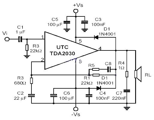
Pin situation:
1. The pin is the positive input terminal.
2. The pin is the reverse input terminal
3. The pin is the negative power input terminal.
4. The pin is the power output terminal
5. Pin is the positive power input terminal.
Precautions:
1. TDA2030 has a load discharge voltage kickback protection circuit. If the peak voltage of the power supply voltage is 40V, an LC filter must be inserted between pin 5 and the power supply to ensure that the pulse train on pin 5 is maintained within the specified amplitude.
2. Thermal protection: Thermal limit protection has the following advantages. It can easily withstand output overload (even for a long time) or protect when the ambient temperature exceeds.
3. Compared with ordinary circuits, the heat sink can have a smaller safety factor. In case the junction temperature exceeds, there will be no damage to the device. If this happens, Po = (and of course Ptot) and Io will be reduced.
4. When designing the printed circuit board, the decoupling of the ground wire and the output must be well considered, because these lines have large currents flowing through them.
5. During assembly, there is no need for insulation between the heat sink and the heat sink, the lead length should be as short as possible, and the welding temperature should not exceed 260°C for 12 seconds.
6. Although TDA2030 requires very few components, the components selected must be of guaranteed quality.
- Field effect tube amplifier circuit with beautiful sound
- Single-ended Class A amplifier using gallstone composite tube design
- Design and production of NE5532+TDA1521 amplifier
- The production of 6P14 small tube amplifier
- Typical applications of optocouplers in audio amplifier circuits
- Class AB2 Amplifier-McIntosh MC80
- High gain audio amplifier circuit composed of LM4818
- Auxiliary audio power amplifier circuit using LM4732
- Multimedia Hi-Fi amplifier circuit
- LM4906 Audio Power Amplifier Circuit
- Typical audio signal control circuit diagram
- Audio Dynamic Noise Cancellation System
- Circuit diagram of low power headphone amplifier made with NE5532
- NE5532 designed HIFI headphone amplifier circuit diagram
- Five-digit LED display audio power indication circuit diagram made with FD502
- SCA (background music) decoder circuit diagram
- Application circuit of TDA2030 - single power supply operation
- 555 sound and light audio circuit
- 555 police car audio circuit
- Rhythm-changing audio circuit


 京公网安备 11010802033920号