Load transient response test of voltage regulator (2)
Source: InternetPublisher:常思一二 Keywords: Voltage regulator load transient response Updated: 2025/09/30
Bipolar transistors
The circuit in Figure 8 greatly simplifies the loop dynamics of the previous circuit and eliminates all AC trimming. The main trade-off is a halving of speed. This circuit is similar to the one in Figure 6, except that Q1 is a bipolar transistor. The bipolar's significantly reduced input capacitance allows A1 to drive more benign loads. This approach allows you to use an amplifier with lower output current and eliminates the dynamic adjustments required to accommodate the gate capacitance of the FET in Figure 6. The only adjustment is a 1-mV adjustment, which you perform as described. You eliminate this trimming at the expense of circuit complexity. In addition to a two-fold speed reduction, the bipolar transistor introduces a 1% output current error due to its base current. You add Q2 to prevent excessive Q1 base current when no regulator power is present. This diode prevents reverse base bias under all conditions.
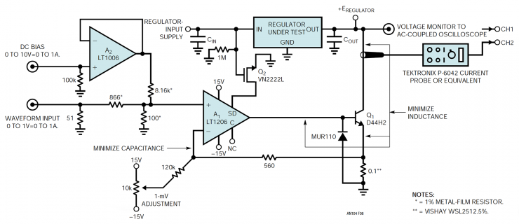
Figure 8 This circuit matches Figure 6, but with a bipolar transistor. Q1's reduced input capacitance simplifies the loop dynamics, eliminating compensation components and trimming. The trade-off is halved speed and a 1% error due to base current.
Closed-loop circuit performance
Figures 9 and 10 illustrate the operation of the two broadband circuits. The FET-based circuit (Figure 9) requires only a 50-mV A1 swing (Trace A) to force the flat-top current pulse (Trace B) through Q1 with a 50-ns edge. Figure 10 details the performance of the bipolar transistor-based circuit. Trace A, taken from the base of Q1, rises less than 100 mV, resulting in a clean 1A current (Trace B) being conducted through Q1. This circuit's 100-nanosecond edge is roughly twice as slow as the more complex FET-based version, but is still fast enough for most practical transient load tests.
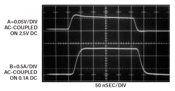
Figure 9: The closed-loop load tester step response of Figure 6 is fast and clean, showing a 50-nanosecond edge and a flat top. (Q1's current is trace B.) A1's output (trace A) swings only 50 mV, allowing for wideband operation. Trace B is presented with a slight delay due to the time skew of the voltage and current probes.
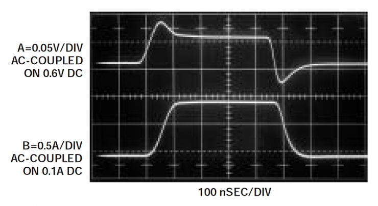
Figure 10 The bipolar output load tester of Figure 8 responds twice as slowly as the FET version, but the circuit is simpler and requires no compensation trimming. Trace A is the output of A1, and Trace B is the collector current of Q1.
Load transient test
These circuits allow for quick and thorough load transient testing of voltage regulators. Figure 11 uses the circuit of Figure 6 to evaluate the LT1963A linear regulator. Figure 12 shows the regulator's response to an asymmetric input pulse on Trace A (Trace B). A ramping rising edge within the LT1963A's bandwidth results in a smooth 10mVpp excursion on Trace B. A fast trailing edge, far outside the LT1963A's passband, causes an abrupt discontinuity in Trace B. Cout supplies too little current to maintain the output level, and a 75mVpp spike occurs before the regulator regains control. In Figure 13, a 500mApp, 500kHz noise load, simulating a large, incoherent load, is fed into the regulator in Trace A. This frequency is within the regulator's bandwidth, and only a 6mVpp disturbance appears in Trace B (regulator output). Figure 14 maintains the same conditions, except the noise bandwidth is increased to 5MHz. This increase exceeds the regulation bandwidth, resulting in more than 50-mV pp error, an eightfold increase.
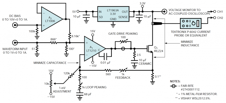
Figure 11. This closed-loop load tester with the LT1963A regulator provides load testing for various current and load waveforms.
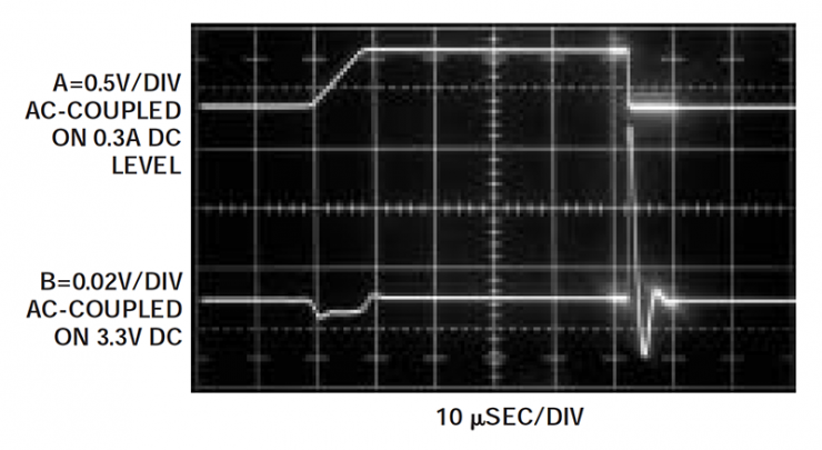
Figure 12 shows the circuit response in Figure 11 (trace B) to an asymmetric edge pulse input (trace A). A ramp leading edge within the LT1963A's bandwidth results in a smooth 10-mV-pp excursion in trace B. A fast falling edge outside the LT1963A's bandwidth causes an abrupt 75-mV-pp discontinuity in trace B. The second half of the trace is emphasized in the photo for clarity.
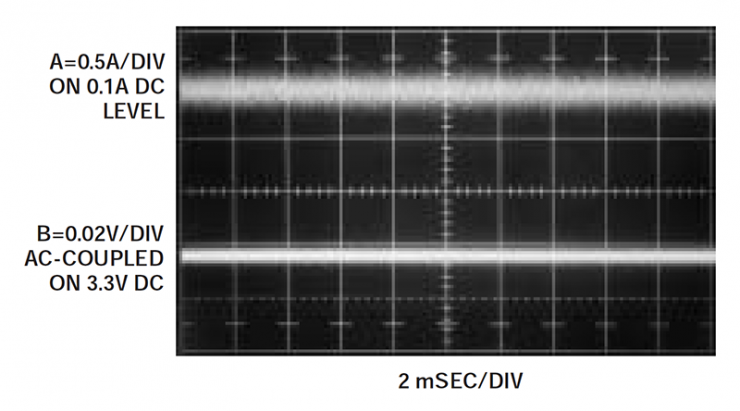
Figure 13. A 500-mA-pp, 500-kHz noise load within the regulator's passband (Trace A) produces only a 6-mV artifact at the regulator's output (Trace B).
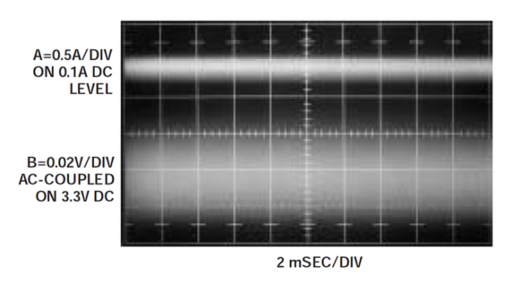
Figure 14 This waveform has the same conditions as Figure 13, except that the noise bandwidth has increased by 5 MHz, exceeding the bandwidth of the regulator and resulting in a 50-mV-pp output error.
Figure 15 shows what happens when you supply 0.2A to the regulator, bias it with DC, and sweep it from DC to 5MHz with a 0.35A load. The increase in the regulator's output impedance with frequency causes the error to increase with frequency. This information allows you to determine the regulator's output impedance vs. frequency.
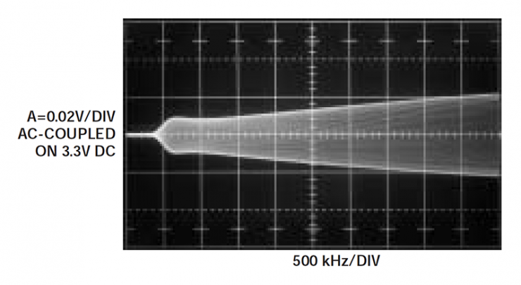
Figure 15. Frequency sweep, DC to 5MHz, 0.35A load on a 0.2A DC load causes the regulator's output impedance to increase with frequency and a corresponding increase in output error.
- Electronic fuse
- Dual-channel adjustable power supply
- Automatic battery charger
- 500W 12V to 220V inverter
- High-current regulated power supply based on LM317
- DC 13.8V to DC 250V inverter circuit
- bidirectional solid-state relay
- Power Tip: What's the best way to drive a synchronous rectifier in a flyback power supply?
- How to simulate our buck converter control loop?
- Re-examining the importance of current power monitors
- Importance of Voltage Supervisors and Output Topology Selection
- Design of adjustable DC stabilized power supply circuit module
- Power circuit of LBO-522 dual trace oscilloscope
- Power circuit with smoothing filter capacitor
- 500A-6V single-phase thyristor voltage regulating electroplating power supply circuit
- 300A-18V three-phase thyristor voltage regulating electrolytic power supply circuit
- Household emergency power circuit
- Inverter power circuit made with BJ50A
- Based on LM117 variable voltage regulator
- 5V voltage regulator circuit


 京公网安备 11010802033920号