Clamping diodes are a one-way street
Source: InternetPublisher:无人共我 Keywords: Power protection clamping diode Updated: 2025/09/30
The most familiar application of the unidirectional conduction characteristic of diodes is diode rectification. A clamping circuit also utilizes this characteristic. Clamping forcibly clamps a signal to a certain potential, raising or lowering the base potential without changing the original signal waveform. This is what clamping is.
“Can I allow input signals when VCC = 0 V?”
“What happens if the input or output voltage drops below GND?”
Customers often ask these questions—and with good reason. Many standard logic datasheets don't explicitly specify conditions where the inputs are above VCC or below ground (GND). The device itself has few, if any, performance characteristics in the datasheet at these marginal voltages.
One of the most important features of most TI devices is electrostatic discharge (ESD) protection. In fact, in some devices, ESD protection circuitry occupies a large portion of the chip real estate. Typically, ESD circuitry includes a diode that diverts excess current to GND (via reverse breakdown) or VCC (via forward bias) when the input voltage approaches unsafe levels. The goal is to prevent damage to the internal circuitry.
However, ESD diodes can have some unexpected effects. For example, if there is an input diode connected from the input to VCC, an input voltage at VCC = 0 will cause current to flow through the device to the VCC pin. Similarly, when the input reaches a certain level below GND, a diode from GND to the input will cause current to flow from GND to the input.
So how do we know when the input diode is present, and how can we prevent the negative effects?
The Absolute Maximum Ratings table (Table 1) contains the answer.
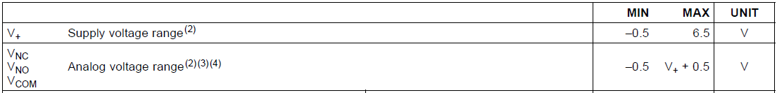 Table 1: Sample Absolute Maximum Ratings Table
On this analog switch, we can see that the voltage on the I/O pin is not allowed to go above VCC or below -0.5 V. Therefore, we can conclude that there is a diode to VCC and a diode from GND on each I/O port of the device.
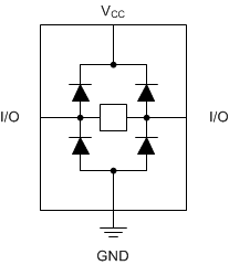
Figure 1: ESD diode structure of the device. The Absolute Max Table is similar to Table 1.
Table 2 provides another example where the absolute maximum rating is structured slightly differently.
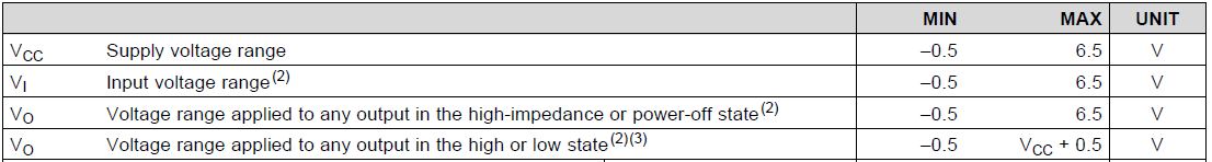 Table 2: Example Absolute Maximum Ratings Table with Different Input and Output Limits
Here, we can see diodes from GND to both the input and output, and an ESD diode to VCC at the output. When the device is in the high or low state, there is a risk of current flowing through the VCC diode. The device has a special feature called a high-impedance state that prevents current from flowing back through the diode. It also has protection circuitry for when VCC = 0, called IOFF.
However, from the VCC + 0.5V statement, we know that there is a diode connected from the output to VCC, and that there is protection circuitry to prevent problems in certain configurations.
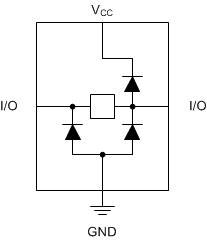
Figure 2: ESD diode structure for a device with absolute maximum ratings similar to those in Table 2
But what are the limits? The specifications IIK and IOK describe the current limits that can flow into the device (positive values) and out of the device (negative values) through the ESD diodes. Consider the first case (Table 3) where we have two GND diodes.
 Table 3: Sample ratings for clamping current in absolute maximum ratings
The current in the GND diode is limited to 50mA. For the second case of the V CC diode, the “Output Clamp Current” will have a +/- sign to indicate that current can flow in both directions (into the V CC diode or out of the GND diode).
It’s best to avoid situations where the ESD diodes might turn on. Most datasheets specify exceptions to the input and output voltage rules – so if we limit the diode clamping current using a series resistor on the input or output, our risk of device damage is greatly reduced.
- TDA1010 9W Power Amplifier
- Infrared proximity sensor
- Digital step-kilometer counter
- Transistor working state: detailed explanation of transistor cutoff region, amplification region and saturation region
- Schottky diode function
- Error Analysis of Practical Operational Amplifier Circuits
- Introduction to the application of open collector output in high current load control circuit
- Some Techniques for Calculating Transistor Amplifier Circuits
- Switched Gain Op Amp as a Phase Detector or Mixer
- Using AD8307 logarithmic amplifier to form a power meter circuit
- DC regulated power supply protection device composed of 555
- Fast action power protection circuit
- Power protection circuit
- Household power protector circuit
- Power protection circuit
- Power protection circuit
- Transient voltage suppressor as DC power supply protection circuit
- Transient voltage suppressor as AC power protection circuit
- 555 square wave oscillation circuit
- 555 photo exposure timer circuit diagram


 京公网安备 11010802033920号