How do I solve the problem of mismatched voltage levels between devices?
Source: InternetPublisher:newlandmark Keywords: Power Converter Updated: 2025/06/27
Single supply converters are becoming an essential device on any board to connect two systems operating at different voltage levels. The input threshold of the conversion solution (V il , V ih ) should be within the output level of the driver (V ol , Voh) and similarly, the output of the solution (V ol , V oh ) should be within the valid input threshold of the receiver (V i , V ih ).
Designers can implement the voltage conversion using either a single supply converter or dual supply converters.
Examples of single-supply converters include the SN74AUP1T and SN74LV1T.
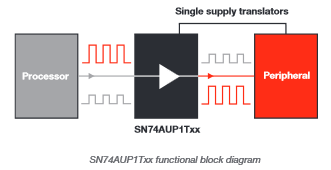
Figure 1: Functional block diagram of a single-supply converter
These devices have a single supply voltage that essentially tracks the peripheral supply voltage, as shown in Figure 1. The input ports have overvoltage tolerance, which allows them to act as step-down converters. Up-conversion occurs at compatible Vih - Vil levels relative to Vcc. The input signal must swing above Vih and below Vil for up-conversion to occur.
The Advanced Ultra Low Power CMOS (AUP) family is optimized for low power consumption of approximately 0.5uA, while the SN74LVT family of devices has a wide operating range of 1.8V to 5.5V. Open-drain devices allow flexible conversion to a voltage determined by the pull-up resistor, but there is a problem of constant current flow when the output voltage is low. A low level at the preset (PRE) or clear (CUR) input sets or resets the output regardless of the levels of the other inputs. When PRE and CLR are inactive (high), data at the data (D) input that meets the setup time requirements is transferred to the output on the positive edge of the clock pulse. The clock trigger occurs at the voltage level and is not directly related to the rise time of the clock pulse. After the hold time interval, the data at the D input can be changed without affecting the output level.
Higher current consumption is always an issue when using a single supply converter for conversion, which becomes critical when operating in power-sensitive applications, as shown in Figure 2.
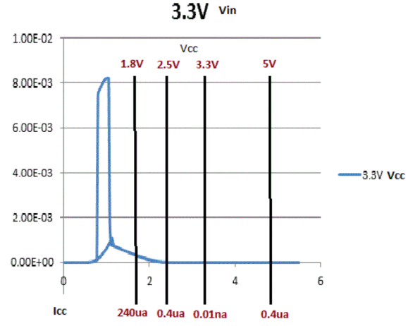
Figure 2: Power consumption analysis
The delta I cc spec in the datasheet is the difference in current draw for each input that is not on one of the rails. When Vin is about mid-point of Vcc, the delta I cc spec is highest, in mA.
A dual-supply converter device essentially has two independent supplies: one that tracks the input port and another that tracks the peripheral that requires voltage conversion, as shown in Figure 3.
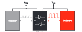
Figure 3: Dual-supply converter with V CCA and V CCB
Dual-supply converters fall into different categories: bidirectional (LSF, Gunning Transistor Logic [GTL]), automatic direction sensing (TXB, TXS), and direction configurable (AVCT, LVCT).
The bidirectional converter allows conversion on either of its two ports acting as input or output. The core of the LSF is a passive field effect transistor (FET) switch that converts between any two voltage levels using an external pull-up resistor. The LSF is suitable for high-speed open-drain and push-pull applications with an overall range of 1V to 5V and no direction terminal required. The GTL series of devices are suitable for low-voltage applications and can convert 3.6V low-voltage transistor-transistor logic (LVTTL) to GTL logic.
The automatic direction-sensing switch eliminates the need for a separate input for direction control, thereby reducing software development costs and associated synchronization issues.
The TXB010x and TXB030x devices are targeted for push-pull applications with fast edge rates, while the TXS010x / -E is targeted for open-drain applications. Both the TXB010x and TXS010x / -E family devices feature a partial power-off I off feature. Figure 4 shows the relationship between the conversion capability of the TXB010x / TXS010x device family and the bit widths available in the TI portfolio.
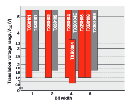
Figure 4: Analysis of an automatic direction sensing converter
Direction Control Converters have a separate direction control pin that determines the direction of communication. Whenever data transfer is bidirectional, there is potential bus contention, which can be eliminated using the direction control of these devices. Figure 5 compares the bit widths offered versus the conversion voltage. The AVC1T45 device operates over a voltage range of 1.2V to 3.6V, while the LVC1T45 device operates over a wider voltage range of 1.65V to 5.5V. As Ioff is a common feature of these devices, they provide Vcc isolation, where the port is in high impedance mode when either Vcc is at ground potential.
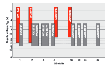
Figure 5: Analysis of a configurable direction-controlled converter
Unidirectional converters such as the AVC2T245 feature dual supplies that track two independent voltages configurable from 0.9V to 3.6V for low-power battery use. TI's Crossbar Technology (CBT) and Transition Voltage Clamp (TVC) families feature down-conversion capabilities for specific switching applications.
Unmatched voltage levels between devices can create problems that can be mitigated by using single or dual supply converters. Have we had to use one recently? If so, how did we use voltage translation in our designs? After reading all the options presented, would we use the same translation method in our next application?
- 5V power supply with overvoltage protection
- +5V power supply for charge pump battery charger
- LM317 Adjustable Regulated Power Supply
- 500W 12V to 220V inverter
- TL431 Lithium-ion Charger
- Fluorescent lamp inverter
- High-current regulated power supply based on LM317
- 10A 1-30V Adjustable Power Supply Based on LM317
- Top Three Ways to Split Voltage Rails into Bipolar Power Supplies
- When debugging a boost converter, you can analyze it from four directions.
- 24V power supply pure flat display high voltage power supply circuit diagram
- DC 12V to AC 100V inverter power supply circuit design
- 300A-18V three-phase thyristor voltage regulating electrolytic power supply circuit
- Single LTC power circuit
- Karaoke light controller circuit (1)
- Neon light high voltage power supply circuit
- Common power circuits and applications 06
- Common power circuits and applications 02
- ±5V, ±12V power circuit A
- 6.3V, 270V, 300V DC power supply circuit


 京公网安备 11010802033920号