CD4060 AC power adapter with timed shutdown
Source: InternetPublisher:拳制龙 Keywords: CD4060 timing power supply circuit Updated: 2024/07/10
Many people like to lie in bed reading books, newspapers, listening to the radio, and enjoying music. They often fall asleep unconsciously, which causes the bedside lamp to be on all night or other electrical appliances to work all night. The power adapter with timing function made by the author can solve the above problem well.
The circuit is shown in the figure below. Press the micro switch button AN, and the 220V AC power supply will be reduced by the transformer and rectified by the diode bridge to obtain a 9V DC voltage. The voltage is stabilized by the voltage regulator integrated block LM7805, and the working voltage of the timing clock generator composed of the CD4060 integrated circuit is supplied. At the same time, the 5V voltage after voltage regulation is further reduced by three series-connected diodes to output a voltage of about 3V, which can be used as a DC regulated power supply for portable radios, walkmans, etc. The two-position selection switch SW is used to convert the output polarity of the DC regulated power supply. The light-emitting diode LED is the power working indicator.
At the beginning of power-on, the timing clock generator is first reset by the capacitor of IC{12} pin, and each output stage is at low potential. Since the output terminal Q14 outputs a low level, the transistor VT1 is cut off, VT2 is turned on, the relay J is energized, and the contacts are closed. AC OUT is an AC output socket, which can be used as a bedside lighting, a miniature ceiling fan, and other AC appliances that require timing but have no timing control.
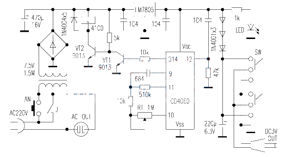
The CD4060 integrated circuit is a 14-level binary counter/distributor with an internal clock pulse oscillator. The external resistors and capacitors at the {9} and {10} pins determine the oscillation frequency of the clock. The timing time can be changed by adjusting the potentiometer RT. The value marked in the figure indicates that the timing time is approximately between 20 seconds and 4.5 hours. When the timing clock generator counts and distributes the output of the high level to the Q14 terminal, the transistor VT1 changes from the original cut-off to the on state, and VT2 changes from the on state to the cut-off state; the relay J loses power and the contact is released, cutting off the AC input power supply, and the whole machine stops working immediately.
This circuit can be successful without debugging as long as the components are correct and the soldering is correct.
- Analysis of the working principle of switching regulator
- 5 Converter Topologies for Integrated Solar and Storage Systems
- How to Make a Soft Latch Circuit
- Introduction and principle analysis of switching regulated power supply
- Basic circuit description of adjustable voltage regulator LM317
- Use pulse width modulation to get a precise output voltage
- Parallel DC regulated power supply circuit diagram
- How to use SBR to improve power conversion efficiency
- Using CW34603 to form a circuit to change the polarity of the output power supply
- Homemade low-power UPS
- 3v to 5v circuit diagram
- Commonly used power circuits in printers
- 2-phase CPU power supply circuit using HIP6302 and HIP6602 chips
- Transistor stabilized current power supply circuit 2
- DC power supply circuit for semiconductor radio
- Power circuit for home appliance repair
- Common power circuits and applications 09
- Common power circuits and applications 08
- Always ready power circuit
- ±5V, ±12V power circuit A


 京公网安备 11010802033920号