3551J amplifier basic information:
3551J is an OPERATIONAL AMPLIFIER. The commonly used packaging method is CAN8,.2
3551J amplifier core information:
The minimum operating temperature of the 3551J is 70 °C. Its peak reflow temperature is NOT SPECIFIED Its maximum bias current at 25°C is: 0.0004 µA Its maximum average bias current is 0.0004 µA
How to simply check the efficiency of an amplifier? Looking at its slew rate, the nominal slew rate of 3551J is 250 V/us. The maximum slew rate of the 3551J given by the manufacturer is 15 mA. Its minimum voltage gain is 25000. When the op amp is used in a closed loop, at a certain closed-loop gain (usually 1 or 2, 10, etc.), the frequency when the 3551J gain becomes 0.707 times the low-frequency gain is 50,000 kHz.
The nominal supply voltage of the 3551J is 15 V, and its corresponding nominal negative supply voltage is -15 V. The power supply range is: +-15 V. The input offset voltage of 3551J is 1000 µV (input offset voltage: the compensation voltage added between the two input terminals to make the output terminal of the operational amplifier 0V (or close to 0V).)
Related dimensions of 3551J:
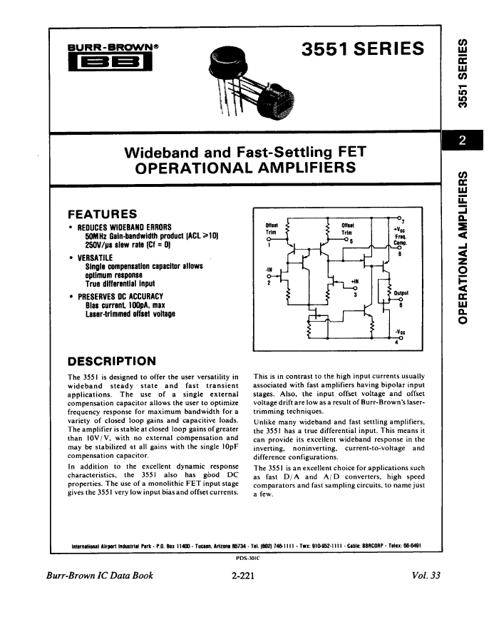
3551J has 8 terminals. Its terminal position type is: BOTTOM.
3551J amplifier additional information:
3551J adopts the VOLTAGE-FEEDBACK architecture. It belongs to the low-bias class of amplifiers. It does not belong to the low offset class of amplifiers. The frequency compensation status of 3551J is: YES (AVCL>=10). Its temperature grade is: COMMERCIAL.
3551J is not Rohs certified. The corresponding JESD-30 code is: O-MBCY-W8. The corresponding JESD-609 code is: e0. The material of the 3551J package is mostly METAL. And its package shape is ROUND.
The 3551J package pin forms are: CYLINDRICAL. Its terminal form is: WIRE.
3551J amplifier basic information:
3551J is an OPERATIONAL AMPLIFIER. The commonly used packaging method is CAN8,.2
3551J amplifier core information:
The minimum operating temperature of the 3551J is 70 °C. Its peak reflow temperature is NOT SPECIFIED Its maximum bias current at 25°C is: 0.0004 µA Its maximum average bias current is 0.0004 µA
How to simply check the efficiency of an amplifier? Looking at its slew rate, the nominal slew rate of 3551J is 250 V/us. The maximum slew rate of the 3551J given by the manufacturer is 15 mA. Its minimum voltage gain is 25000. When the op amp is used in a closed loop, at a certain closed-loop gain (usually 1 or 2, 10, etc.), the frequency when the 3551J gain becomes 0.707 times the low-frequency gain is 50,000 kHz.
The nominal supply voltage of the 3551J is 15 V, and its corresponding nominal negative supply voltage is -15 V. The power supply range is: +-15 V. The input offset voltage of 3551J is 1000 µV (input offset voltage: the compensation voltage added between the two input terminals to make the output terminal of the operational amplifier 0V (or close to 0V).)
Related dimensions of 3551J:
3551J has 8 terminals. Its terminal position type is: BOTTOM.
3551J amplifier additional information:
3551J adopts the VOLTAGE-FEEDBACK architecture. It belongs to the low-bias class of amplifiers. It does not belong to the low offset class of amplifiers. The frequency compensation status of 3551J is: YES (AVCL>=10). Its temperature grade is: COMMERCIAL.
3551J is not Rohs certified. The corresponding JESD-30 code is: O-MBCY-W8. The corresponding JESD-609 code is: e0. The material of the 3551J package is mostly METAL. And its package shape is ROUND.
The 3551J package pin forms are: CYLINDRICAL. Its terminal form is: WIRE.
| Parameter Name | Attribute value |
| Is it Rohs certified? | incompatible |
| package instruction | , CAN8,.2 |
| Reach Compliance Code | unknown |
| Amplifier type | OPERATIONAL AMPLIFIER |
| Architecture | VOLTAGE-FEEDBACK |
| Maximum average bias current (IIB) | 0.0004 µA |
| Maximum bias current (IIB) at 25C | 0.0004 µA |
| Nominal Common Mode Rejection Ratio | 70 dB |
| frequency compensation | YES (AVCL>=10) |
| Maximum input offset voltage | 1000 µV |
| JESD-30 code | O-MBCY-W8 |
| JESD-609 code | e0 |
| low-bias | YES |
| low-dissonance | NO |
| Nominal Negative Supply Voltage (Vsup) | -15 V |
| Number of functions | 1 |
| Number of terminals | 8 |
| Maximum operating temperature | 70 °C |
| Minimum operating temperature | |
| Package body material | METAL |
| Encapsulate equivalent code | CAN8,.2 |
| Package shape | ROUND |
| Package form | CYLINDRICAL |
| Peak Reflow Temperature (Celsius) | NOT SPECIFIED |
| power supply | +-15 V |
| Certification status | Not Qualified |
| Nominal slew rate | 250 V/us |
| Maximum slew rate | 15 mA |
| Supply voltage upper limit | 20 V |
| Nominal supply voltage (Vsup) | 15 V |
| surface mount | NO |
| technology | BIPOLAR |
| Temperature level | COMMERCIAL |
| Terminal surface | Tin/Lead (Sn/Pb) |
| Terminal form | WIRE |
| Terminal location | BOTTOM |
| Maximum time at peak reflow temperature | NOT SPECIFIED |
| Nominal Uniform Gain Bandwidth | 50000 kHz |
| Minimum voltage gain | 25000 |
| Base Number Matches | 1 |
| 3551J | 3551S | |
|---|---|---|
| Description | Operational Amplifier, 1 Func, 1000uV Offset-Max, BIPolar, MBCY8, TO-99, 8 PIN | Operational Amplifier, 1 Func, 1000uV Offset-Max, BIPolar, MBCY8, TO-99, 8 PIN |
| Is it Rohs certified? | incompatible | incompatible |
| package instruction | , CAN8,.2 | , CAN8,.2 |
| Reach Compliance Code | unknown | unknown |
| Amplifier type | OPERATIONAL AMPLIFIER | OPERATIONAL AMPLIFIER |
| Architecture | VOLTAGE-FEEDBACK | VOLTAGE-FEEDBACK |
| Maximum average bias current (IIB) | 0.0004 µA | 0.0004 µA |
| Maximum bias current (IIB) at 25C | 0.0004 µA | 0.0004 µA |
| Nominal Common Mode Rejection Ratio | 70 dB | 70 dB |
| frequency compensation | YES (AVCL>=10) | YES (AVCL>=10) |
| Maximum input offset voltage | 1000 µV | 1000 µV |
| JESD-30 code | O-MBCY-W8 | O-MBCY-W8 |
| JESD-609 code | e0 | e0 |
| low-bias | YES | YES |
| low-dissonance | NO | NO |
| Nominal Negative Supply Voltage (Vsup) | -15 V | -15 V |
| Number of functions | 1 | 1 |
| Number of terminals | 8 | 8 |
| Maximum operating temperature | 70 °C | 125 °C |
| Package body material | METAL | METAL |
| Encapsulate equivalent code | CAN8,.2 | CAN8,.2 |
| Package shape | ROUND | ROUND |
| Package form | CYLINDRICAL | CYLINDRICAL |
| Peak Reflow Temperature (Celsius) | NOT SPECIFIED | NOT SPECIFIED |
| power supply | +-15 V | +-15 V |
| Certification status | Not Qualified | Not Qualified |
| Nominal slew rate | 250 V/us | 250 V/us |
| Maximum slew rate | 15 mA | 15 mA |
| Supply voltage upper limit | 20 V | 20 V |
| Nominal supply voltage (Vsup) | 15 V | 15 V |
| surface mount | NO | NO |
| technology | BIPOLAR | BIPOLAR |
| Temperature level | COMMERCIAL | MILITARY |
| Terminal surface | Tin/Lead (Sn/Pb) | Tin/Lead (Sn/Pb) |
| Terminal form | WIRE | WIRE |
| Terminal location | BOTTOM | BOTTOM |
| Maximum time at peak reflow temperature | NOT SPECIFIED | NOT SPECIFIED |
| Nominal Uniform Gain Bandwidth | 50000 kHz | 50000 kHz |
| Minimum voltage gain | 25000 | 25000 |
 京公网安备 11010802033920号


