5962R9853301V9A amplifier basic information:
5962R9853301V9A is an OPERATIONAL AMPLIFIER. Commonly used packaging methods are DIE, DIE OR CHIP
5962R9853301V9A amplifier core information:
The minimum operating temperature of 5962R9853301V9A is -55 °C and the maximum operating temperature is 125 °C. Its peak reflow temperature is NOT SPECIFIED Its maximum bias current at 25°C is: 0.63 µA Its maximum average bias current is 0.63 µA
How to simply check the efficiency of an amplifier? Looking at its slew rate, the nominal slew rate of 5962R9853301V9A is 1.7 V/us. The minimum slew rate of 5962R9853301V9A given by the manufacturer is 1.2 V/us. Its minimum voltage gain is 40000. When the op amp is used in closed loop, at a certain closed-loop gain (usually 1 or 2, 10, etc.), the frequency when the gain of 5962R9853301V9A becomes 0.707 times the low-frequency gain is 8000 kHz.
The nominal supply voltage of 5962R9853301V9A is 15 V, and its corresponding nominal negative supply voltage is -15 V. The input offset voltage of 5962R9853301V9A is 2100 µV (input offset voltage: the compensation voltage added between the two input terminals to make the output terminal of the operational amplifier 0V (or close to 0V).)
Related dimensions of 5962R9853301V9A:
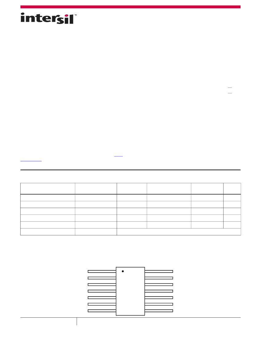
5962R9853301V9A has 14 terminals. Its terminal position type is: UPPER. Total pins: 14
5962R9853301V9A amplifier other information:
5962R9853301V9A adopts the VOLTAGE-FEEDBACK architecture. It does not belong to the low offset class of amplifiers. The frequency compensation status of 5962R9853301V9A is: YES. Its temperature grade is: MILITARY. 5962R9853301V9A does not comply with Rohs certification.
It does not contain lead. The corresponding JESD-30 code is: R-XUUC-N14. The corresponding JESD-609 code is: e4. The packaging code of 5962R9853301V9A is: DIE. The materials used in the 5962R9853301V9A package are mostly UNSPECIFIED.
The package shape is RECTANGULAR. The 5962R9853301V9A package pin format is: UNCASED CHIP. Its terminal forms are: NO LEAD.
5962R9853301V9A amplifier basic information:
5962R9853301V9A is an OPERATIONAL AMPLIFIER. Commonly used packaging methods are DIE, DIE OR CHIP
5962R9853301V9A amplifier core information:
The minimum operating temperature of 5962R9853301V9A is -55 °C and the maximum operating temperature is 125 °C. Its peak reflow temperature is NOT SPECIFIED Its maximum bias current at 25°C is: 0.63 µA Its maximum average bias current is 0.63 µA
How to simply check the efficiency of an amplifier? Looking at its slew rate, the nominal slew rate of 5962R9853301V9A is 1.7 V/us. The minimum slew rate of 5962R9853301V9A given by the manufacturer is 1.2 V/us. Its minimum voltage gain is 40000. When the op amp is used in closed loop, at a certain closed-loop gain (usually 1 or 2, 10, etc.), the frequency when the gain of 5962R9853301V9A becomes 0.707 times the low-frequency gain is 8000 kHz.
The nominal supply voltage of 5962R9853301V9A is 15 V, and its corresponding nominal negative supply voltage is -15 V. The input offset voltage of 5962R9853301V9A is 2100 µV (input offset voltage: the compensation voltage added between the two input terminals to make the output terminal of the operational amplifier 0V (or close to 0V).)
Related dimensions of 5962R9853301V9A:
5962R9853301V9A has 14 terminals. Its terminal position type is: UPPER. Total pins: 14
5962R9853301V9A amplifier other information:
5962R9853301V9A adopts the VOLTAGE-FEEDBACK architecture. It does not belong to the low offset class of amplifiers. The frequency compensation status of 5962R9853301V9A is: YES. Its temperature grade is: MILITARY. 5962R9853301V9A does not comply with Rohs certification.
It does not contain lead. The corresponding JESD-30 code is: R-XUUC-N14. The corresponding JESD-609 code is: e4. The packaging code of 5962R9853301V9A is: DIE. The materials used in the 5962R9853301V9A package are mostly UNSPECIFIED.
The package shape is RECTANGULAR. The 5962R9853301V9A package pin format is: UNCASED CHIP. Its terminal forms are: NO LEAD.
| Parameter Name | Attribute value |
| Is it lead-free? | Lead free |
| Is it Rohs certified? | incompatible |
| Maker | Renesas Electronics Corporation |
| Parts packaging code | DIE |
| package instruction | DIE, DIE OR CHIP |
| Contacts | 14 |
| Reach Compliance Code | not_compliant |
| ECCN code | USML XV(E) |
| Amplifier type | OPERATIONAL AMPLIFIER |
| Architecture | VOLTAGE-FEEDBACK |
| Maximum average bias current (IIB) | 0.63 µA |
| Maximum bias current (IIB) at 25C | 0.63 µA |
| Nominal Common Mode Rejection Ratio | 80 dB |
| frequency compensation | YES |
| Maximum input offset voltage | 2100 µV |
| JESD-30 code | R-XUUC-N14 |
| JESD-609 code | e4 |
| low-dissonance | NO |
| Negative supply voltage upper limit | -20 V |
| Nominal Negative Supply Voltage (Vsup) | -15 V |
| Number of functions | 4 |
| Number of terminals | 14 |
| Maximum operating temperature | 125 °C |
| Minimum operating temperature | -55 °C |
| Package body material | UNSPECIFIED |
| encapsulated code | DIE |
| Encapsulate equivalent code | DIE OR CHIP |
| Package shape | RECTANGULAR |
| Package form | UNCASED CHIP |
| Peak Reflow Temperature (Celsius) | NOT SPECIFIED |
| power supply | +-5/+-15 V |
| Certification status | Not Qualified |
| Filter level | MIL-PRF-38535 Class V |
| minimum slew rate | 1.2 V/us |
| Nominal slew rate | 1.7 V/us |
| Supply voltage upper limit | 20 V |
| Nominal supply voltage (Vsup) | 15 V |
| surface mount | YES |
| technology | BIPOLAR |
| Temperature level | MILITARY |
| Terminal surface | Gold (Au) |
| Terminal form | NO LEAD |
| Terminal location | UPPER |
| Maximum time at peak reflow temperature | NOT SPECIFIED |
| total dose | 100k Rad(Si) V |
| Nominal Uniform Gain Bandwidth | 8000 kHz |
| Minimum voltage gain | 40000 |
| Base Number Matches | 1 |
 京公网安备 11010802033920号


