E2G0029-17-41
¡ Semiconductor
MSM519200
¡ Semiconductor
This version: Jan. 1998
MSM519200
Previous version: May 1997
4,194,304-Word
¥
2-Bit DYNAMIC RAM : FAST PAGE MODE TYPE
DESCRIPTION
The MSM519200 is a 4,194,304-word
¥
2-bit dynamic RAM fabricated in Oki's silicon-gate CMOS
technology. The MSM519200 achieves high integration, high-speed operation, and low-power
consumption because Oki manufactures the device in a quadruple-layer polysilicon/double-layer
metal CMOS process. The MSM519200 is available in a 26/24-pin plastic SOJ or 26/24-pin plastic
TSOP.
FEATURES
• 4,194,304-word
¥
2-bit configuration
• Single 5 V power supply,
±10%
tolerance
• Input
: TTL compatible, low input capacitance
• Output : TTL compatible, 3-state
• Refresh : 2048 cycles/32 ms
• Fast page mode, read modify write capability
•
CAS
before
RAS
refresh, hidden refresh,
RAS-only
refresh capability
• Multi-bit test mode capability
• Package options:
26/24-pin 300 mil plastic SOJ (SOJ26/24-P-300-1.27) (Product : MSM519200-xxSJ)
26/24-pin 300 mil plastic TSOP (TSOPII26/24-P-300-1.27-K) (Product : MSM519200-xxTS-K)
xx indicates speed rank.
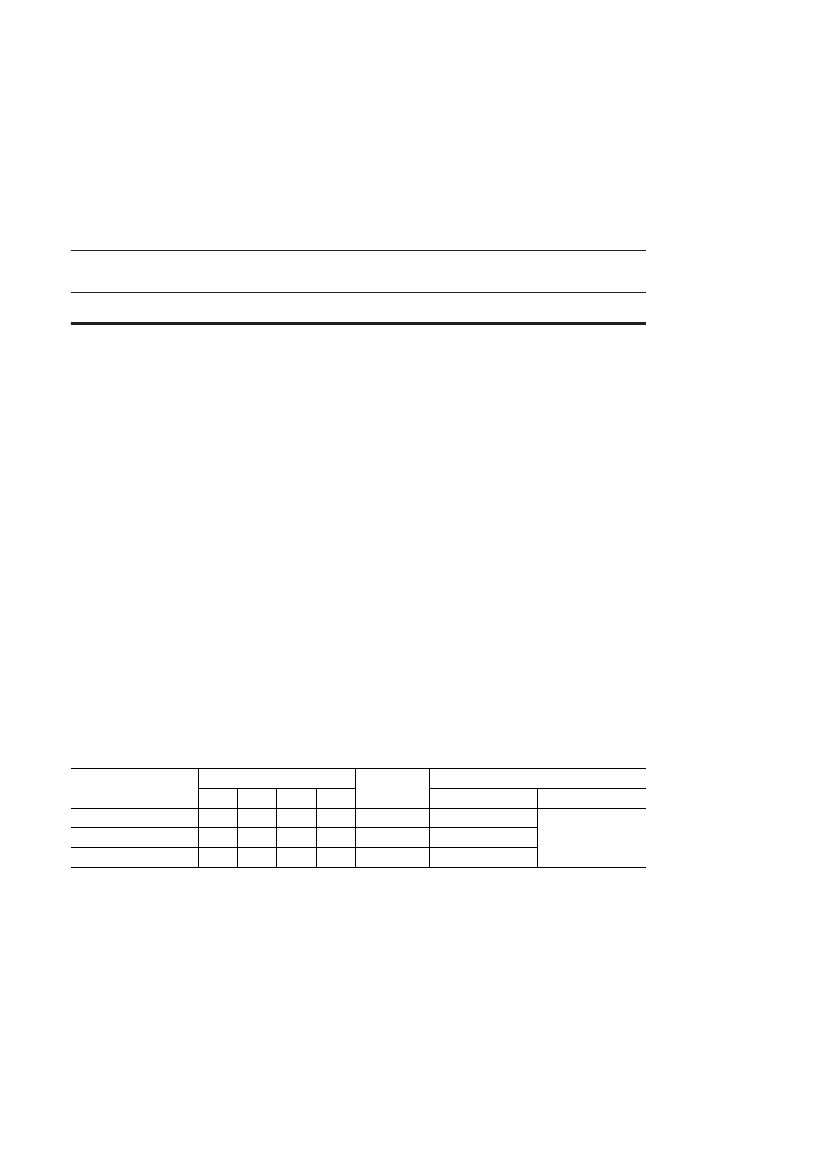
PRODUCT FAMILY
Family
MSM519200-60
MSM519200-70
MSM519200-80
Access Time (Max.)
t
RAC
t
AA
t
CAC
t
OEA
60 ns 30 ns 15 ns 15 ns
70 ns 35 ns 20 ns 20 ns
80 ns 40 ns 20 ns 20 ns
Cycle Time
Power Dissipation
(Min.)
Operating (Max.) Standby (Max.)
110 ns
130 ns
150 ns
440 mW
413 mW
385 mW
5.5 mW
1/17
¡ Semiconductor
PIN CONFIGURATION (TOP VIEW)
V
CC
1
��
26 V
SS
25 NC
V
CC
1
DQ1 2
WE
4
NC 6
DQ1 2
WE
4
NC 6
DQ2 3
24
CAS1
23
CAS2
22
OE
21 A9
DQ2 3
RAS
5
RAS
5
A10 8
A0 9
19 A8
A10 8
18 A7
17 A6
16 A5
15 A4
14 V
SS
A0 9
A1 10
A2 11
A3 12
V
CC
13
A1 10
A2 11
A3 12
V
CC
13
26/24-Pin Plastic SOJ
Pin Name
A0 - A10
RAS
CAS1, CAS2
DQ1, DQ2
OE
WE
V
CC
V
SS
NC
Function
Address Input
Row Address Strobe
Column Address Strobe
Data Input/Data Output
Output Enable
Write Enable
Power Supply (5 V)
Ground (0 V)
No Connection
MSM519200
26 V
SS
25 NC
24
CAS1
23
CAS2
22
OE
21 A9
19 A8
18 A7
17 A6
16 A5
15 A4
14 V
SS
26/24-Pin Plastic TSOP
(K Type)
Note :
The same power supply voltage must be provided to every V
CC
pin, and the same GND
voltage level must be provided to every V
SS
pin.
2/17
¡ Semiconductor
MSM519200
ELECTRICAL CHARACTERISTICS
Absolute Maximum Ratings
Parameter
Voltage on Any Pin Relative to V
SS
Short Circuit Output Current
Power Dissipation
Operating Temperature
Storage Temperature
Symbol
V
T
I
OS
P
D
*
T
opr
T
stg
Rating
–1.0 to 7.0
50
1
0 to 70
–55 to 150
Unit
V
mA
W
°C
°C
*: Ta = 25°C
Recommended Operating Conditions
Parameter
Power Supply Voltage
Input High Voltage
Input Low Voltage
Symbol
V
CC
V
SS
V
IH
V
IL
Min.
4.5
0
2.4
–1.0
Typ.
5.0
0
—
—
Max.
5.5
0
6.5
0.8
(Ta = 0°C to 70°C)
Unit
V
V
V
V
Capacitance
Parameter
Input Capacitance (A0 - A10)
Input Capacitance
(RAS,
CAS1, CAS2, WE, OE)
Output Capacitance (DQ1, DQ2)
Symbol
C
IN1
C
IN2
C
I/O
Typ.
—
—
—
(V
CC
= 5 V ±10%, Ta = 25°C, f = 1 MHz)
Max.
6
7
10
Unit
pF
pF
pF
4/17
¡ Semiconductor
DC Characteristics
Parameter
Output High Voltage
Output Low Voltage
Input Leakage Current
Condition
MSM519200
(V
CC
= 5 V ±10%, Ta = 0°C to 70°C)
Symbol
MSM519200 MSM519200 MSM519200
-60
-70
-80
Unit Note
Min.
Max.
V
CC
0.4
10
Min.
2.4
0
–10
Max.
V
CC
0.4
10
Min.
2.4
0
–10
Max.
V
CC
0.4
10
V
V
mA
2.4
0
–10
V
OH
I
OH
= –5.0 mA
V
OL
I
OL
= 4.2 mA
0 V
£
V
I
£
6.5 V;
I
LI
All other pins not
under test = 0 V
DQ disable
0 V
£
V
O
£
5.5 V
RAS, CAS1, CAS2
I
CC1
cycling,
t
RC
= Min.
RAS, CAS1, CAS2
= V
IH
I
CC2
RAS, CAS1, CAS2
≥
V
CC
–0.2 V
RAS
cycling,
I
CC3
CAS1, CAS2
= V
IH
,
t
RC
= Min.
RAS
= V
IH
,
I
CC5
CAS1, CAS2
= V
IL
,
DQ = enable
RAS
cycling,
I
CC6
CAS1, CAS2
before
RAS
RAS
= V
IL
,
I
CC7
CAS1, CAS2
cycling,
t
PC
= Min.
Output Leakage Current
Average Power
Supply Current
(Operating)
Power Supply
Current (Standby)
Average Power
Supply Current
(RAS-only Refresh)
Power Supply
Current (Standby)
Average Power
Supply Current
(CAS before
RAS
Refresh)
Average Power
Supply Current
(Fast Page Mode)
I
LO
–10
10
–10
10
–10
10
mA
—
—
—
80
2
1
—
—
—
75
2
1
—
—
—
70
2
1
mA 1, 2
mA
1
—
80
—
75
—
70
mA 1, 2
—
5
—
5
—
5
mA
1
—
80
—
75
—
70
mA 1, 2
—
70
—
65
—
60
mA 1, 3
Notes : 1. I
CC
Max. is specified as I
CC
for output open condition.
2. The address can be changed once or less while
RAS
= V
IL
.
3. The address can be changed once or less while
CAS1, CAS2
= V
IH
.
5/17
 京公网安备 11010802033920号


