
Silicon PNP epitaxial planer type(For power amplification)
| Parameter Name | Attribute value |
| Is it Rohs certified? | conform to |
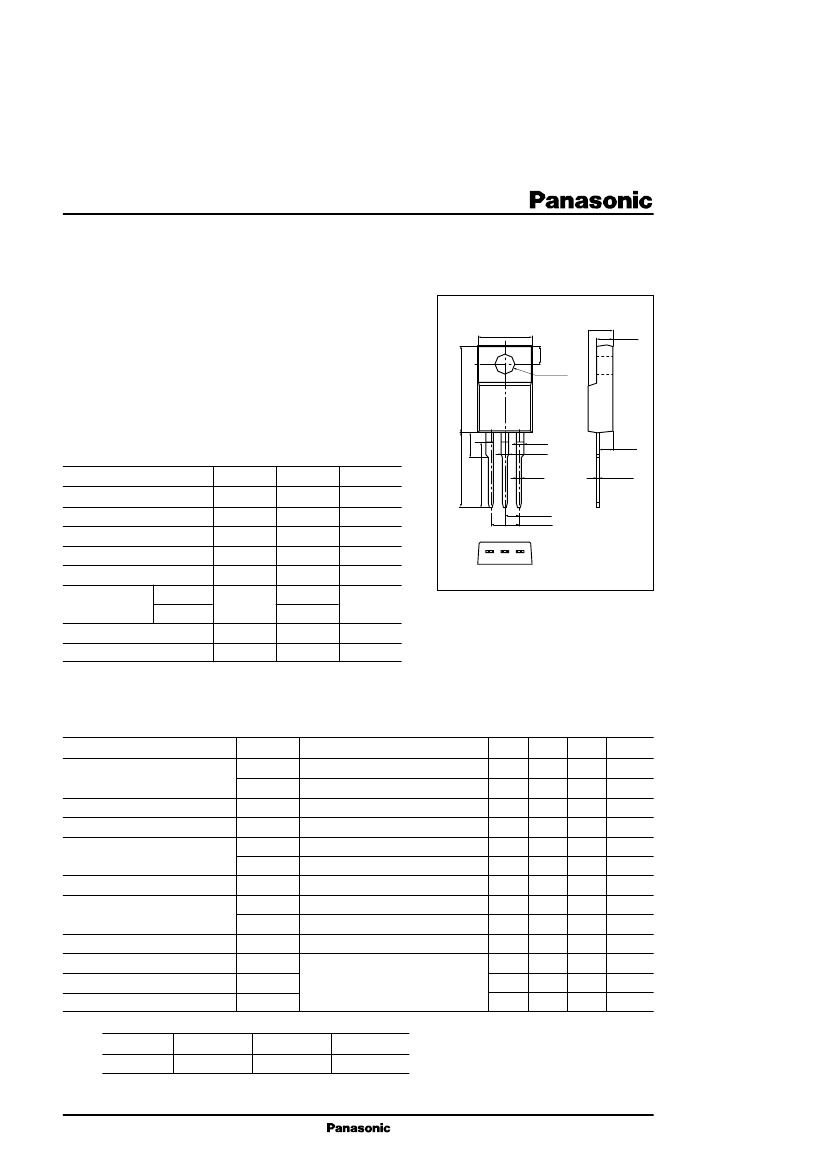
| Parts packaging code | TO-220AB |
| package instruction | ROHS COMPLIANT, TO-220D-A1, 3 PIN |
| Contacts | 3 |
| Reach Compliance Code | unknow |
| ECCN code | EAR99 |
| Shell connection | ISOLATED |
| Maximum collector current (IC) | 4 A |
| Collector-emitter maximum voltage | 60 V |
| Configuration | SINGLE |
| Minimum DC current gain (hFE) | 1000 |
| JEDEC-95 code | TO-220AB |
| JESD-30 code | R-PSFM-T3 |
| JESD-609 code | e6 |
| Humidity sensitivity level | 1 |
| Number of components | 1 |
| Number of terminals | 3 |
| Package body material | PLASTIC/EPOXY |
| Package shape | RECTANGULAR |
| Package form | FLANGE MOUNT |
| Peak Reflow Temperature (Celsius) | 260 |
| Polarity/channel type | PNP |
| Certification status | Not Qualified |
| surface mount | NO |
| Terminal surface | Tin/Bismuth (Sn/Bi) |
| Terminal form | THROUGH-HOLE |
| Terminal location | SINGLE |
| Maximum time at peak reflow temperature | 10 |
| transistor applications | AMPLIFIER |
| Transistor component materials | SILICON |
| Nominal transition frequency (fT) | 20 MHz |
| Base Number Matches | 1 |
 京公网安备 11010802033920号


