Basic information of TLC279MN amplifier:
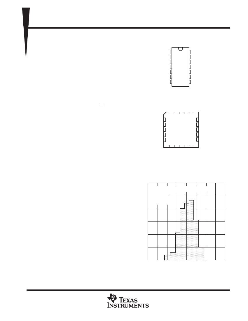
TLC279MN is an OPERATIONAL AMPLIFIER. The commonly used packaging method is DIP,
TLC279MN amplifier core information:
The minimum operating temperature of the TLC279MN is -40 °C and the maximum operating temperature is 85 °C. Its maximum average bias current is 0.00006 µA
How to simply check the efficiency of an amplifier? Looking at its slew rate, the TLC279MN has a nominal slew rate of 2.9 V/us. When the op amp is used in a closed loop, at a certain closed-loop gain (usually 1 or 2, 10, etc.), the frequency when the TLC279MN gain becomes 0.707 times the low-frequency gain is 1700 kHz.
The nominal supply voltage of the TLC279MN is 5 V. The upper limit of its supply voltage is 18. The input offset voltage of VTLC279MN is 3750 µV (input offset voltage: the compensation voltage added between the two input terminals to make the output terminal of the operational amplifier 0V (or close to 0V).)
Related dimensions of TLC279MN:
The width of TLC279MN is: 7.62 mm and the length is 19.305 mm. TLC279MN has 14 terminals. Its terminal position type is: DUAL. Terminal pitch is 2.54 mm.
TLC279MN amplifier additional information:
Its temperature grade is: INDUSTRIAL. The corresponding JESD-30 code is: R-PDIP-T14. The packaging code of TLC279MN is: DIP. The materials used for TLC279MN packaging are mostly PLASTIC/EPOXY. The package shape is RECTANGULAR.
The TLC279MN package pin format is: IN-LINE. Its terminal form is: THROUGH-HOLE. The maximum seat height is 5.08 mm.
Basic information of TLC279MN amplifier:
TLC279MN is an OPERATIONAL AMPLIFIER. The commonly used packaging method is DIP,
TLC279MN amplifier core information:
The minimum operating temperature of the TLC279MN is -40 °C and the maximum operating temperature is 85 °C. Its maximum average bias current is 0.00006 µA
How to simply check the efficiency of an amplifier? Looking at its slew rate, the TLC279MN has a nominal slew rate of 2.9 V/us. When the op amp is used in a closed loop, at a certain closed-loop gain (usually 1 or 2, 10, etc.), the frequency when the TLC279MN gain becomes 0.707 times the low-frequency gain is 1700 kHz.
The nominal supply voltage of the TLC279MN is 5 V. The upper limit of its supply voltage is 18. The input offset voltage of VTLC279MN is 3750 µV (input offset voltage: the compensation voltage added between the two input terminals to make the output terminal of the operational amplifier 0V (or close to 0V).)
Related dimensions of TLC279MN:
The width of TLC279MN is: 7.62 mm and the length is 19.305 mm. TLC279MN has 14 terminals. Its terminal position type is: DUAL. Terminal pitch is 2.54 mm.
TLC279MN amplifier additional information:
Its temperature grade is: INDUSTRIAL. The corresponding JESD-30 code is: R-PDIP-T14. The packaging code of TLC279MN is: DIP. The materials used for TLC279MN packaging are mostly PLASTIC/EPOXY. The package shape is RECTANGULAR.
The TLC279MN package pin format is: IN-LINE. Its terminal form is: THROUGH-HOLE. The maximum seat height is 5.08 mm.
| Parameter Name | Attribute value |
| package instruction | DIP, |
| Reach Compliance Code | unknown |
| ECCN code | EAR99 |
| Amplifier type | OPERATIONAL AMPLIFIER |
| Maximum average bias current (IIB) | 0.00006 µA |
| Nominal Common Mode Rejection Ratio | 80 dB |
| Maximum input offset voltage | 3750 µV |
| JESD-30 code | R-PDIP-T14 |
| length | 19.305 mm |
| Number of functions | 4 |
| Number of terminals | 14 |
| Maximum operating temperature | 85 °C |
| Minimum operating temperature | -40 °C |
| Package body material | PLASTIC/EPOXY |
| encapsulated code | DIP |
| Package shape | RECTANGULAR |
| Package form | IN-LINE |
| Maximum seat height | 5.08 mm |
| Nominal slew rate | 2.9 V/us |
| Supply voltage upper limit | 18 V |
| Nominal supply voltage (Vsup) | 5 V |
| surface mount | NO |
| technology | CMOS |
| Temperature level | INDUSTRIAL |
| Terminal form | THROUGH-HOLE |
| Terminal pitch | 2.54 mm |
| Terminal location | DUAL |
| Nominal Uniform Gain Bandwidth | 1700 kHz |
| width | 7.62 mm |
| Base Number Matches | 1 |
| TLC279MN | TLC279MJ | TLC279MFK | |
|---|---|---|---|
| Description | Operational Amplifier, 4 Func, 3750uV Offset-Max, CMOS, PDIP14, PLASTIC, DIP-14 | Operational Amplifier, 4 Func, 3750uV Offset-Max, CMOS, CDIP14, CERAMIC, DIP-14 | Operational Amplifier, 4 Func, 12000uV Offset-Max, CMOS, CQCC20, CERAMIC, LCC-20 |
| package instruction | DIP, | DIP, | HQCCN, |
| Reach Compliance Code | unknown | unknown | unknown |
| ECCN code | EAR99 | EAR99 | EAR99 |
| Amplifier type | OPERATIONAL AMPLIFIER | OPERATIONAL AMPLIFIER | OPERATIONAL AMPLIFIER |
| Maximum average bias current (IIB) | 0.00006 µA | 0.00006 µA | 0.00006 µA |
| Nominal Common Mode Rejection Ratio | 80 dB | 80 dB | 80 dB |
| Maximum input offset voltage | 3750 µV | 3750 µV | 12000 µV |
| JESD-30 code | R-PDIP-T14 | R-GDIP-T14 | S-CQCC-N20 |
| length | 19.305 mm | 19.56 mm | 8.89 mm |
| Number of functions | 4 | 4 | 4 |
| Number of terminals | 14 | 14 | 20 |
| Maximum operating temperature | 85 °C | 125 °C | 125 °C |
| Minimum operating temperature | -40 °C | -55 °C | -55 °C |
| Package body material | PLASTIC/EPOXY | CERAMIC, GLASS-SEALED | CERAMIC, METAL-SEALED COFIRED |
| encapsulated code | DIP | DIP | HQCCN |
| Package shape | RECTANGULAR | RECTANGULAR | SQUARE |
| Package form | IN-LINE | IN-LINE | CHIP CARRIER, HEAT SINK/SLUG |
| Maximum seat height | 5.08 mm | 5.08 mm | 2.03 mm |
| Nominal slew rate | 2.9 V/us | 2.9 V/us | 2.9 V/us |
| Supply voltage upper limit | 18 V | 18 V | 18 V |
| Nominal supply voltage (Vsup) | 5 V | 5 V | 5 V |
| surface mount | NO | NO | YES |
| technology | CMOS | CMOS | CMOS |
| Temperature level | INDUSTRIAL | MILITARY | MILITARY |
| Terminal form | THROUGH-HOLE | THROUGH-HOLE | NO LEAD |
| Terminal pitch | 2.54 mm | 2.54 mm | 1.27 mm |
| Terminal location | DUAL | DUAL | QUAD |
| Nominal Uniform Gain Bandwidth | 1700 kHz | 1700 kHz | 1700 kHz |
| width | 7.62 mm | 7.62 mm | 8.89 mm |
| Base Number Matches | 1 | 1 | 1 |
 京公网安备 11010802033920号


