5962F1222801VXC amplifier basic information:
5962F1222801VXC is an OPERATIONAL AMPLIFIER. Commonly used packaging methods are DFP, FL14,.25
5962F1222801VXC amplifier core information:
The minimum operating temperature of the 5962F1222801VXC is -55 °C and the maximum operating temperature is 125 °C. Its peak reflow temperature is NOT SPECIFIED Its maximum bias current at 25°C is: 0.001 µA Its maximum average bias current is 0.005 µA
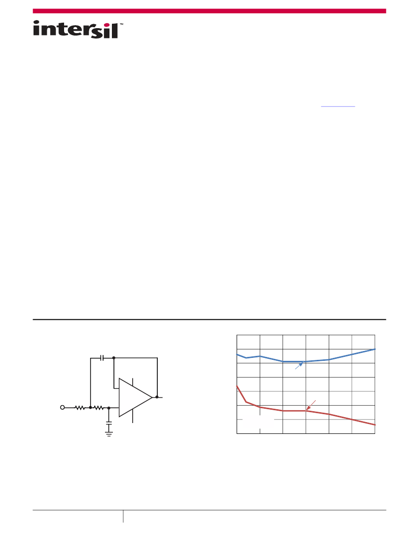
How to simply check the efficiency of an amplifier? Looking at its slew rate, the nominal slew rate of 5962F1222801VXC is 0.5 V/us. The maximum slew rate of the 5962F1222801VXC given by the manufacturer is 2.72 mA, while the minimum slew rate is 0.2 V/us. Its minimum voltage gain is 3000000. When the op amp is used in closed loop, at a certain closed-loop gain (usually 1 or 2, 10, etc.), the frequency when the 5962F1222801VXC gain becomes 0.707 times the low-frequency gain is 1500 kHz.
The nominal supply voltage of 5962F1222801VXC is 5 V, and its corresponding nominal negative supply voltage is -5 V. The input offset voltage of 5962F1222801VXC is 250 µV (Input offset voltage: the compensation voltage added between the two input terminals to make the output terminal of the operational amplifier 0V (or close to 0V).)
Related dimensions of 5962F1222801VXC:
The width of 5962F1222801VXC is: 6.285 mm and the length is 9.91 mm. 5962F1222801VXC has 14 terminals. Its terminal position type is: DUAL. Terminal pitch is 1.27 mm.
5962F1222801VXC amplifier additional information:
5962F1222801VXC adopts the VOLTAGE-FEEDBACK architecture. It belongs to the low offset class of amplifiers. The frequency compensation status of 5962F1222801VXC is: YES. Its temperature grade is: MILITARY. It is a micropower amplifier.
5962F1222801VXC does not comply with Rohs certification. The corresponding JESD-30 code is: R-CDFP-F14. The packaging code of 5962F1222801VXC is: DFP. The materials of 5962F1222801VXC package are mostly CERAMIC, METAL-SEALED COFIRED. The package shape is RECTANGULAR.
The 5962F1222801VXC package pin format is: FLATPACK. Its terminal form is: FLAT. The maximum seat height is 2.92 mm.
5962F1222801VXC amplifier basic information:
5962F1222801VXC is an OPERATIONAL AMPLIFIER. Commonly used packaging methods are DFP, FL14,.25
5962F1222801VXC amplifier core information:
The minimum operating temperature of the 5962F1222801VXC is -55 °C and the maximum operating temperature is 125 °C. Its peak reflow temperature is NOT SPECIFIED Its maximum bias current at 25°C is: 0.001 µA Its maximum average bias current is 0.005 µA
How to simply check the efficiency of an amplifier? Looking at its slew rate, the nominal slew rate of 5962F1222801VXC is 0.5 V/us. The maximum slew rate of the 5962F1222801VXC given by the manufacturer is 2.72 mA, while the minimum slew rate is 0.2 V/us. Its minimum voltage gain is 3000000. When the op amp is used in closed loop, at a certain closed-loop gain (usually 1 or 2, 10, etc.), the frequency when the 5962F1222801VXC gain becomes 0.707 times the low-frequency gain is 1500 kHz.
The nominal supply voltage of 5962F1222801VXC is 5 V, and its corresponding nominal negative supply voltage is -5 V. The input offset voltage of 5962F1222801VXC is 250 µV (Input offset voltage: the compensation voltage added between the two input terminals to make the output terminal of the operational amplifier 0V (or close to 0V).)
Related dimensions of 5962F1222801VXC:
The width of 5962F1222801VXC is: 6.285 mm and the length is 9.91 mm. 5962F1222801VXC has 14 terminals. Its terminal position type is: DUAL. Terminal pitch is 1.27 mm.
5962F1222801VXC amplifier additional information:
5962F1222801VXC adopts the VOLTAGE-FEEDBACK architecture. It belongs to the low offset class of amplifiers. The frequency compensation status of 5962F1222801VXC is: YES. Its temperature grade is: MILITARY. It is a micropower amplifier.
5962F1222801VXC does not comply with Rohs certification. The corresponding JESD-30 code is: R-CDFP-F14. The packaging code of 5962F1222801VXC is: DFP. The materials of 5962F1222801VXC package are mostly CERAMIC, METAL-SEALED COFIRED. The package shape is RECTANGULAR.
The 5962F1222801VXC package pin format is: FLATPACK. Its terminal form is: FLAT. The maximum seat height is 2.92 mm.
| Parameter Name | Attribute value |
| Is it Rohs certified? | incompatible |
| package instruction | DFP, FL14,.25 |
| Reach Compliance Code | _compli |
| ECCN code | USML XV(E) |
| Amplifier type | OPERATIONAL AMPLIFIER |
| Architecture | VOLTAGE-FEEDBACK |
| Maximum average bias current (IIB) | 0.005 µA |
| Maximum bias current (IIB) at 25C | 0.001 µA |
| Nominal Common Mode Rejection Ratio | 145 dB |
| frequency compensation | YES |
| Maximum input offset voltage | 250 µV |
| JESD-30 code | R-CDFP-F14 |
| length | 9.91 mm |
| low-dissonance | YES |
| micropower | YES |
| Negative supply voltage upper limit | -21 V |
| Nominal Negative Supply Voltage (Vsup) | -5 V |
| Number of functions | 4 |
| Number of terminals | 14 |
| Maximum operating temperature | 125 °C |
| Minimum operating temperature | -55 °C |
| Package body material | CERAMIC, METAL-SEALED COFIRED |
| encapsulated code | DFP |
| Encapsulate equivalent code | FL14,.25 |
| Package shape | RECTANGULAR |
| Package form | FLATPACK |
| Peak Reflow Temperature (Celsius) | NOT SPECIFIED |
| power supply | +-5/+-15 V |
| Certification status | Not Qualified |
| Filter level | MIL-PRF-38535 Class V |
| Maximum seat height | 2.92 mm |
| minimum slew rate | 0.2 V/us |
| Nominal slew rate | 0.5 V/us |
| Maximum slew rate | 2.72 mA |
| Supply voltage upper limit | 21 V |
| Nominal supply voltage (Vsup) | 5 V |
| surface mount | YES |
| technology | BIPOLAR |
| Temperature level | MILITARY |
| Terminal form | FLAT |
| Terminal pitch | 1.27 mm |
| Terminal location | DUAL |
| Maximum time at peak reflow temperature | NOT SPECIFIED |
| total dose | 300k Rad(Si) V |
| Nominal Uniform Gain Bandwidth | 1500 kHz |
| Minimum voltage gain | 3000000 |
| width | 6.285 mm |
| Base Number Matches | 1 |
| Part Number | Manufacturer | Description |
|---|---|---|
| ISL70417SEHVF | Renesas(瑞萨电子) | 精密放大器 RADIATION HARDENED PRECISION LOW NOISE OPERATIONAL AMPLIFIER |
| ISL70417SEHF/PROTO | Renesas(瑞萨电子) | 精密放大器 RADIATION HARDENED PRECISION LOW NOISE OPERATIONAL AMPLIFIER |
| 5962R1222801VXC | Renesas(瑞萨电子) | QUAD OP-AMP, 250uV OFFSET-MAX, 1.5MHz BAND WIDTH, CDFP14, ROHS COMPLIANT, HERMETIC SEALED, METAL SEALED, CERAMIC, DFP-14 |
 京公网安备 11010802033920号


