
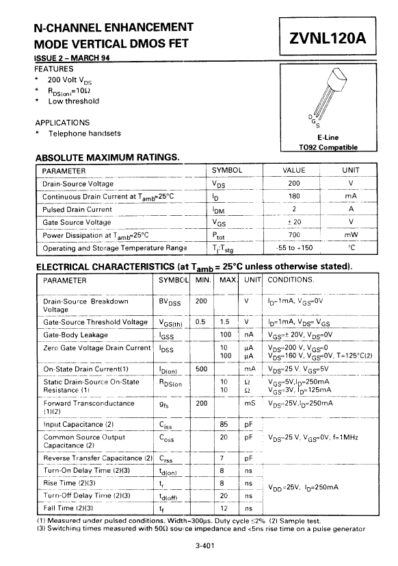
Small Signal Field-Effect Transistor, 0.18A I(D), 200V, 1-Element, N-Channel, Silicon, Metal-oxide Semiconductor FET, TO-92, TO-92 COMPATIBLE, E-LINE PACKAGE-3
| Parameter Name | Attribute value |
| Is it Rohs certified? | conform to |
| Maker | Zetex Semiconductors |
| package instruction | TO-92 COMPATIBLE, E-LINE PACKAGE-3 |
| Reach Compliance Code | not_compliant |
| ECCN code | EAR99 |
| Other features | LOW THRESHOLD |
| Configuration | SINGLE |
| Minimum drain-source breakdown voltage | 200 V |
| Maximum drain current (Abs) (ID) | 0.18 A |
| Maximum drain current (ID) | 0.18 A |
| Maximum drain-source on-resistance | 10 Ω |
| FET technology | METAL-OXIDE SEMICONDUCTOR |
| Maximum feedback capacitance (Crss) | 7 pF |
| JEDEC-95 code | TO-92 |
| JESD-30 code | O-PBCY-W3 |
| JESD-609 code | e3 |
| Humidity sensitivity level | 1 |
| Number of components | 1 |
| Number of terminals | 3 |
| Operating mode | ENHANCEMENT MODE |
| Maximum operating temperature | 200 °C |
| Package body material | PLASTIC/EPOXY |
| Package shape | ROUND |
| Package form | CYLINDRICAL |
| Peak Reflow Temperature (Celsius) | 260 |
| Polarity/channel type | N-CHANNEL |
| Maximum power dissipation(Abs) | 0.7 W |
| Certification status | Not Qualified |
| surface mount | NO |
| Terminal surface | Matte Tin (Sn) |
| Terminal form | WIRE |
| Terminal location | BOTTOM |
| Maximum time at peak reflow temperature | 40 |
| transistor applications | SWITCHING |
| Transistor component materials | SILICON |
| Base Number Matches | 1 |
 京公网安备 11010802033920号


