

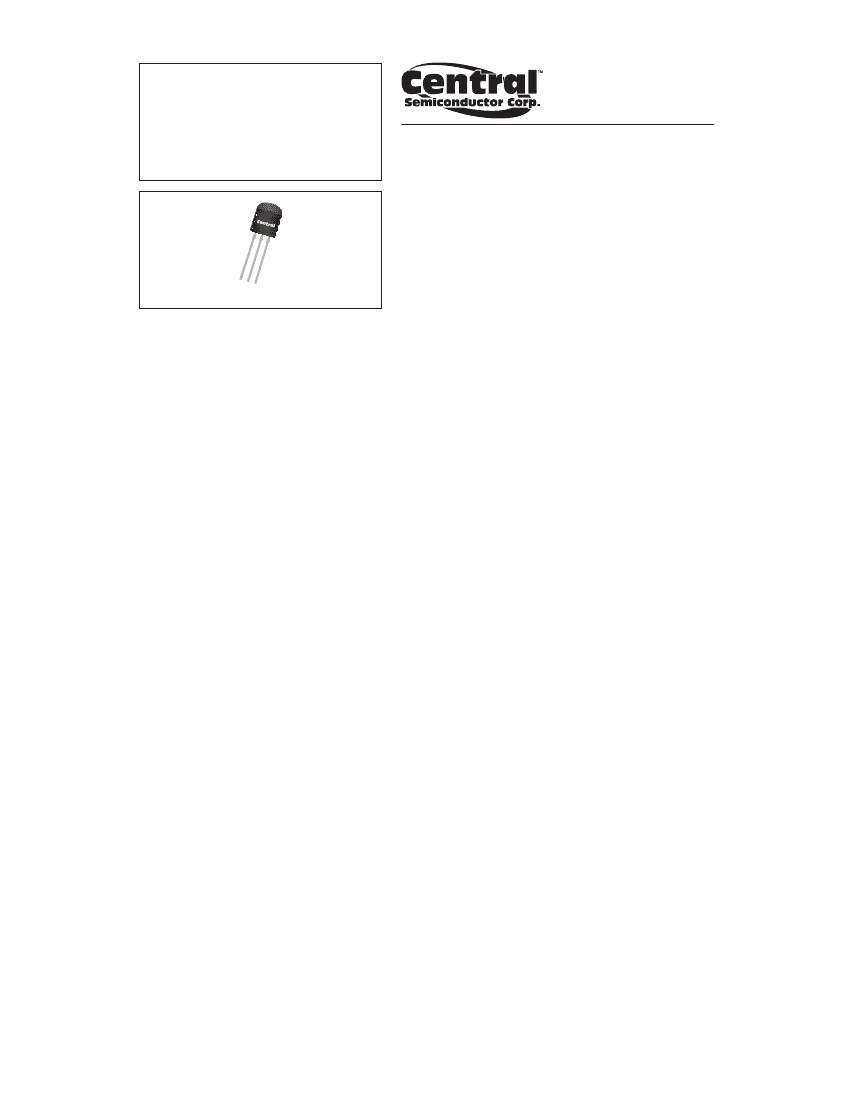
RF Small Signal Bipolar Transistor, 0.05A I(C), 1-Element, Silicon, NPN, TO-92,
| Parameter Name | Attribute value |
| Is it lead-free? | Lead free |
| Is it Rohs certified? | conform to |
| Maker | Central Semiconductor |
| Reach Compliance Code | not_compliant |
| ECCN code | EAR99 |
| Maximum collector current (IC) | 0.05 A |
| Collector-based maximum capacity | 3 pF |
| Collector-emitter maximum voltage | 15 V |
| Configuration | SINGLE |
| JEDEC-95 code | TO-92 |
| JESD-30 code | O-PBCY-T3 |
| JESD-609 code | e3 |
| Number of components | 1 |
| Number of terminals | 3 |
| Package body material | PLASTIC/EPOXY |
| Package shape | ROUND |
| Package form | CYLINDRICAL |
| Peak Reflow Temperature (Celsius) | 260 |
| Polarity/channel type | NPN |
| Certification status | Not Qualified |
| surface mount | NO |
| Terminal surface | MATTE TIN (315) |
| Terminal form | THROUGH-HOLE |
| Terminal location | BOTTOM |
| Maximum time at peak reflow temperature | 10 |
| transistor applications | AMPLIFIER |
| Transistor component materials | SILICON |
| Nominal transition frequency (fT) | 600 MHz |
 京公网安备 11010802033920号


