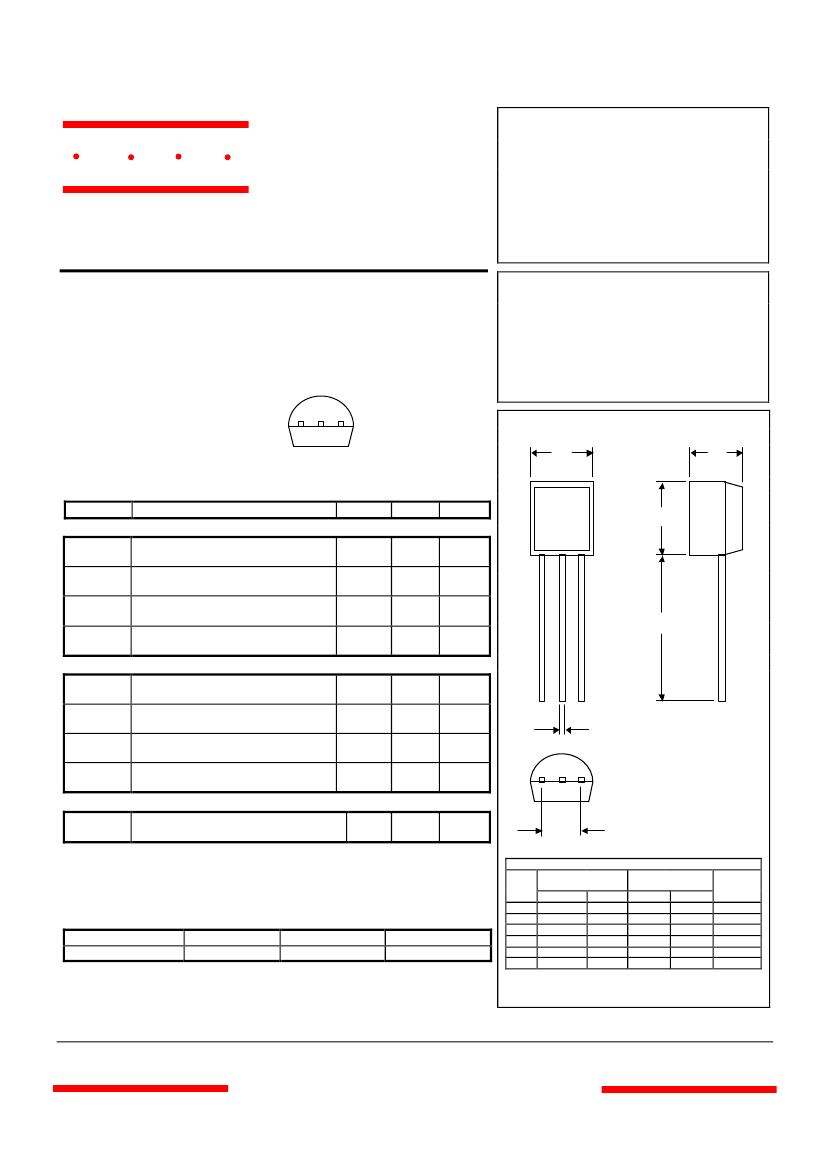
150mA, 50V, PNP, Si, SMALL SIGNAL TRANSISTOR, TO-92, PLASTIC PACKAGE-3
| Parameter Name | Attribute value |
| Is it Rohs certified? | incompatible |
| Parts packaging code | TO-92 |
| package instruction | CYLINDRICAL, O-PBCY-T3 |
| Contacts | 3 |
| Reach Compliance Code | compli |
| Maximum collector current (IC) | 0.15 A |
| Collector-emitter maximum voltage | 50 V |
| Configuration | SINGLE |
| Minimum DC current gain (hFE) | 200 |
| JEDEC-95 code | TO-92 |
| JESD-30 code | O-PBCY-T3 |
| JESD-609 code | e0 |
| Number of components | 1 |
| Number of terminals | 3 |
| Package body material | PLASTIC/EPOXY |
| Package shape | ROUND |
| Package form | CYLINDRICAL |
| Peak Reflow Temperature (Celsius) | NOT SPECIFIED |
| Polarity/channel type | PNP |
| Certification status | Not Qualified |
| surface mount | NO |
| Terminal surface | TIN LEAD |
| Terminal form | THROUGH-HOLE |
| Terminal location | BOTTOM |
| Maximum time at peak reflow temperature | NOT SPECIFIED |
| Transistor component materials | SILICON |
| Nominal transition frequency (fT) | 80 MHz |
| Base Number Matches | 1 |
| 2SA1015GR | 2SA1015Y | 2SA1015O | 2SA1015 | |
|---|---|---|---|---|
| Description | 150mA, 50V, PNP, Si, SMALL SIGNAL TRANSISTOR, TO-92, PLASTIC PACKAGE-3 | 150mA, 50V, PNP, Si, SMALL SIGNAL TRANSISTOR, TO-92, PLASTIC PACKAGE-3 | 150 mA, 50 V, PNP, Si, SMALL SIGNAL TRANSISTOR, TO-92, PLASTIC PACKAGE-3 | Small Signal Bipolar Transistor, 0.15A I(C), 50V V(BR)CEO, 1-Element, PNP, Silicon, TO-92, PLASTIC PACKAGE-3 |
| Is it Rohs certified? | incompatible | incompatible | incompatible | incompatible |
| Parts packaging code | TO-92 | TO-92 | TO-92 | TO-92 |
| package instruction | CYLINDRICAL, O-PBCY-T3 | PLASTIC PACKAGE-3 | CYLINDRICAL, O-PBCY-T3 | CYLINDRICAL, O-PBCY-T3 |
| Contacts | 3 | 3 | 3 | 3 |
| Reach Compliance Code | compli | compli | compli | compliant |
| Maximum collector current (IC) | 0.15 A | 0.15 A | 0.15 A | 0.15 A |
| Collector-emitter maximum voltage | 50 V | 50 V | 50 V | 50 V |
| Configuration | SINGLE | SINGLE | SINGLE | SINGLE |
| Minimum DC current gain (hFE) | 200 | 120 | 70 | 70 |
| JEDEC-95 code | TO-92 | TO-92 | TO-92 | TO-92 |
| JESD-30 code | O-PBCY-T3 | O-PBCY-T3 | O-PBCY-T3 | O-PBCY-T3 |
| JESD-609 code | e0 | e0 | e0 | e0 |
| Number of components | 1 | 1 | 1 | 1 |
| Number of terminals | 3 | 3 | 3 | 3 |
| Package body material | PLASTIC/EPOXY | PLASTIC/EPOXY | PLASTIC/EPOXY | PLASTIC/EPOXY |
| Package shape | ROUND | ROUND | ROUND | ROUND |
| Package form | CYLINDRICAL | CYLINDRICAL | CYLINDRICAL | CYLINDRICAL |
| Peak Reflow Temperature (Celsius) | NOT SPECIFIED | NOT SPECIFIED | NOT SPECIFIED | NOT SPECIFIED |
| Polarity/channel type | PNP | PNP | PNP | PNP |
| Certification status | Not Qualified | Not Qualified | Not Qualified | Not Qualified |
| surface mount | NO | NO | NO | NO |
| Terminal surface | TIN LEAD | TIN LEAD | TIN LEAD | TIN LEAD |
| Terminal form | THROUGH-HOLE | THROUGH-HOLE | THROUGH-HOLE | THROUGH-HOLE |
| Terminal location | BOTTOM | BOTTOM | BOTTOM | BOTTOM |
| Maximum time at peak reflow temperature | NOT SPECIFIED | NOT SPECIFIED | NOT SPECIFIED | NOT SPECIFIED |
| Transistor component materials | SILICON | SILICON | SILICON | SILICON |
| Nominal transition frequency (fT) | 80 MHz | 80 MHz | 80 MHz | 80 MHz |
| Base Number Matches | 1 | 1 | 1 | 1 |
 京公网安备 11010802033920号


