
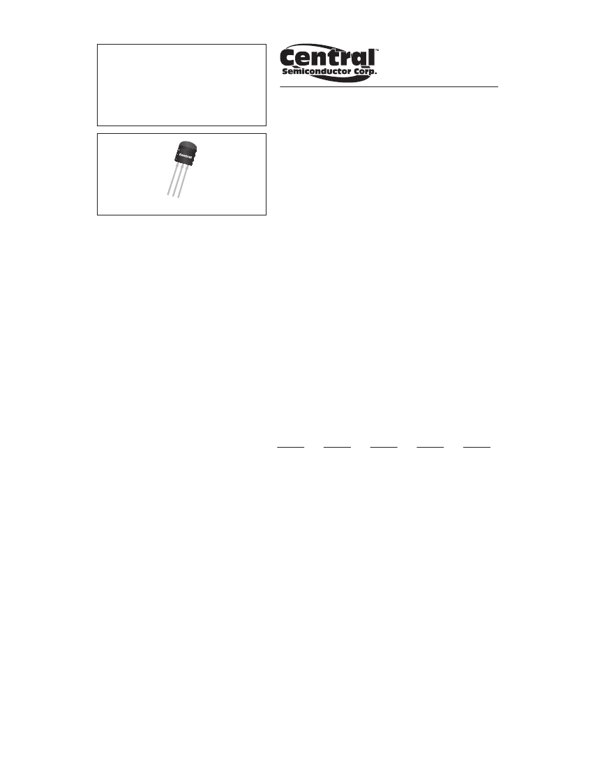
Small Signal Bipolar Transistor, 0.2A I(C), 30V V(BR)CEO, 1-Element, NPN, Silicon, TO-92, TO-92, 3 PIN
| Parameter Name | Attribute value |
| Is it lead-free? | Lead free |
| Is it Rohs certified? | conform to |
| Parts packaging code | TO-92 |
| package instruction | TO-92, 3 PIN |
| Contacts | 3 |
| Reach Compliance Code | _compli |
| ECCN code | EAR99 |
| Other features | LOW NOISE |
| Maximum collector current (IC) | 0.2 A |
| Collector-emitter maximum voltage | 30 V |
| Configuration | SINGLE |
| Minimum DC current gain (hFE) | 180 |
| JEDEC-95 code | TO-92 |
| JESD-30 code | O-PBCY-T3 |
| JESD-609 code | e3 |
| Number of components | 1 |
| Number of terminals | 3 |
| Package body material | PLASTIC/EPOXY |
| Package shape | ROUND |
| Package form | CYLINDRICAL |
| Peak Reflow Temperature (Celsius) | 260 |
| Polarity/channel type | NPN |
| Certification status | Not Qualified |
| surface mount | NO |
| Terminal surface | MATTE TIN (315) |
| Terminal form | THROUGH-HOLE |
| Terminal location | BOTTOM |
| Maximum time at peak reflow temperature | 10 |
| Transistor component materials | SILICON |
| Base Number Matches | 1 |
| 2N3711LEADFREE | 2N3707LEADFREE | 2N3708LEADFREE | 2N3709LEADFREE | 2N3710LEADFREE | |
|---|---|---|---|---|---|
| Description | Small Signal Bipolar Transistor, 0.2A I(C), 30V V(BR)CEO, 1-Element, NPN, Silicon, TO-92, TO-92, 3 PIN | Small Signal Bipolar Transistor, 0.2A I(C), 30V V(BR)CEO, 1-Element, NPN, Silicon, TO-92, TO-92, 3 PIN | Small Signal Bipolar Transistor, 0.2A I(C), 30V V(BR)CEO, 1-Element, NPN, Silicon, TO-92, TO-92, 3 PIN | Small Signal Bipolar Transistor, 0.2A I(C), 30V V(BR)CEO, 1-Element, NPN, Silicon, TO-92, TO-92, 3 PIN | Small Signal Bipolar Transistor, 0.2A I(C), 30V V(BR)CEO, 1-Element, NPN, Silicon, TO-92, TO-92, 3 PIN |
| Is it lead-free? | Lead free | Lead free | Lead free | Lead free | Lead free |
| Is it Rohs certified? | conform to | conform to | conform to | conform to | conform to |
| Parts packaging code | TO-92 | TO-92 | TO-92 | TO-92 | TO-92 |
| package instruction | TO-92, 3 PIN | TO-92, 3 PIN | TO-92, 3 PIN | TO-92, 3 PIN | TO-92, 3 PIN |
| Contacts | 3 | 3 | 3 | 3 | 3 |
| Reach Compliance Code | _compli | _compli | _compli | _compli | _compli |
| ECCN code | EAR99 | EAR99 | EAR99 | EAR99 | EAR99 |
| Other features | LOW NOISE | LOW NOISE | LOW NOISE | LOW NOISE | LOW NOISE |
| Maximum collector current (IC) | 0.2 A | 0.2 A | 0.2 A | 0.2 A | 0.2 A |
| Collector-emitter maximum voltage | 30 V | 30 V | 30 V | 30 V | 30 V |
| Configuration | SINGLE | SINGLE | SINGLE | SINGLE | SINGLE |
| Minimum DC current gain (hFE) | 180 | 100 | 45 | 45 | 90 |
| JEDEC-95 code | TO-92 | TO-92 | TO-92 | TO-92 | TO-92 |
| JESD-30 code | O-PBCY-T3 | O-PBCY-T3 | O-PBCY-T3 | O-PBCY-T3 | O-PBCY-T3 |
| JESD-609 code | e3 | e3 | e3 | e3 | e3 |
| Number of components | 1 | 1 | 1 | 1 | 1 |
| Number of terminals | 3 | 3 | 3 | 3 | 3 |
| Package body material | PLASTIC/EPOXY | PLASTIC/EPOXY | PLASTIC/EPOXY | PLASTIC/EPOXY | PLASTIC/EPOXY |
| Package shape | ROUND | ROUND | ROUND | ROUND | ROUND |
| Package form | CYLINDRICAL | CYLINDRICAL | CYLINDRICAL | CYLINDRICAL | CYLINDRICAL |
| Peak Reflow Temperature (Celsius) | 260 | 260 | 260 | 260 | 260 |
| Polarity/channel type | NPN | NPN | NPN | NPN | NPN |
| Certification status | Not Qualified | Not Qualified | Not Qualified | Not Qualified | Not Qualified |
| surface mount | NO | NO | NO | NO | NO |
| Terminal surface | MATTE TIN (315) | MATTE TIN (315) | MATTE TIN (315) | MATTE TIN (315) | MATTE TIN (315) |
| Terminal form | THROUGH-HOLE | THROUGH-HOLE | THROUGH-HOLE | THROUGH-HOLE | THROUGH-HOLE |
| Terminal location | BOTTOM | BOTTOM | BOTTOM | BOTTOM | BOTTOM |
| Maximum time at peak reflow temperature | 10 | 10 | 10 | 10 | 10 |
| Transistor component materials | SILICON | SILICON | SILICON | SILICON | SILICON |
| Base Number Matches | 1 | 1 | 1 | 1 | 1 |
 京公网安备 11010802033920号


