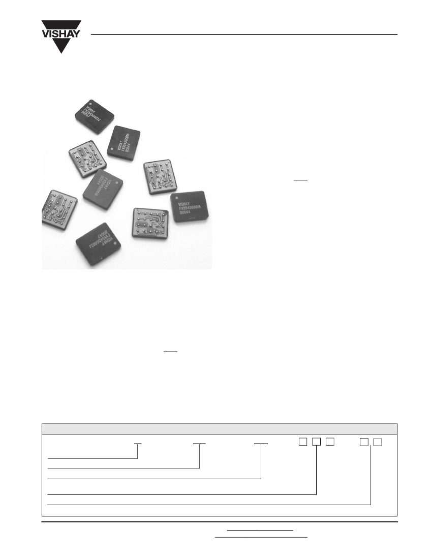
DC-DC Booster Module, 1 Output, 5W, Hybrid, BGA-20
| Parameter Name | Attribute value |
| Is it Rohs certified? | incompatible |
| Maker | Vishay |
| Parts packaging code | MODULE |
| package instruction | BGA, BGA20,4X5,100 |
| Contacts | 20 |
| Reach Compliance Code | unknown |
| ECCN code | EAR99 |
| Analog Integrated Circuits - Other Types | DC-DC BOOSTER MODULE |
| Maximum input voltage | 6 V |
| Minimum input voltage | 2.5 V |
| Nominal input voltage | 3.5 V |
| JESD-30 code | R-XBGA-B20 |
| JESD-609 code | e0 |
| length | 14.7 mm |
| Number of functions | 1 |
| Output times | 1 |
| Number of terminals | 20 |
| Maximum operating temperature | 85 °C |
| Minimum operating temperature | -40 °C |
| Maximum output current | 1 A |
| Maximum output voltage | 5.15 V |
| Minimum output voltage | 4.85 V |
| Nominal output voltage | 5 V |
| Package body material | UNSPECIFIED |
| encapsulated code | BGA |
| Encapsulate equivalent code | BGA20,4X5,100 |
| Package shape | RECTANGULAR |
| Package form | GRID ARRAY |
| Peak Reflow Temperature (Celsius) | NOT SPECIFIED |
| Certification status | Not Qualified |
| Maximum seat height | 3 mm |
| surface mount | YES |
| technology | HYBRID |
| Temperature level | INDUSTRIAL |
| Terminal surface | Tin/Lead (Sn/Pb) |
| Terminal form | BALL |
| Terminal pitch | 2.54 mm |
| Terminal location | BOTTOM |
| Maximum time at peak reflow temperature | NOT SPECIFIED |
| Maximum total power output | 5 W |
| Fine-tuning/adjustable output | NO |
| width | 12.2 mm |
| FX5545G4025V0T2 | FX5545G4023V3T2E2 | FX5545G4025V0B5 | FX5545G402ADJB1E2 | FX5545G402ADJT2E2 | FX5545G402ADJB5E2 | 3623_18 | FX5545G4026V0T1E2 | FX5545G4026V0B5E2 | FX5545G4025V0B1E2 | |
|---|---|---|---|---|---|---|---|---|---|---|
| Description | DC-DC Booster Module, 1 Output, 5W, Hybrid, BGA-20 | DC-DC Booster Module, 1 Output, 5W, Hybrid, LEAD FREE, BGA-20 | DC-DC Booster Module, 1 Output, 5W, Hybrid, BGA-20 | DC-DC Booster Module, 1 Output, 5W, Hybrid, LEAD FREE, BGA-20 | DC-DC Booster Module, 1 Output, 5W, Hybrid, LEAD FREE, BGA-20 | DC-DC Booster Module, 1 Output, 5W, Hybrid, LEAD FREE, BGA-20 | RAST 5 connectors, pitch 5.0 mm | DC-DC Booster Module, 1 Output, 5W, Hybrid, LEAD FREE, BGA-20 | DC-DC Booster Module, 1 Output, 5W, Hybrid, LEAD FREE, BGA-20 | DC-DC Booster Module, 1 Output, 5W, Hybrid, LEAD FREE, BGA-20 |
| Is it Rohs certified? | incompatible | conform to | incompatible | conform to | conform to | conform to | - | conform to | conform to | conform to |
| Maker | Vishay | Vishay | Vishay | Vishay | Vishay | Vishay | - | Vishay | Vishay | Vishay |
| Parts packaging code | MODULE | MODULE | MODULE | MODULE | MODULE | MODULE | - | MODULE | MODULE | MODULE |
| package instruction | BGA, BGA20,4X5,100 | BGA, BGA20,4X5,100 | BGA, BGA20,4X5,100 | BGA, BGA20,4X5,100 | BGA, BGA20,4X5,100 | BGA, BGA20,4X5,100 | - | BGA, BGA20,4X5,100 | BGA, BGA20,4X5,100 | BGA, BGA20,4X5,100 |
| Contacts | 20 | 20 | 20 | 20 | 20 | 20 | - | 20 | 20 | 20 |
| Reach Compliance Code | unknown | unknown | unknown | unknown | unknown | unknown | - | unknown | unknown | unknown |
| ECCN code | EAR99 | EAR99 | EAR99 | EAR99 | EAR99 | EAR99 | - | EAR99 | EAR99 | EAR99 |
| Analog Integrated Circuits - Other Types | DC-DC BOOSTER MODULE | DC-DC BOOSTER MODULE | DC-DC BOOSTER MODULE | DC-DC BOOSTER MODULE | DC-DC BOOSTER MODULE | DC-DC BOOSTER MODULE | - | DC-DC BOOSTER MODULE | DC-DC BOOSTER MODULE | DC-DC BOOSTER MODULE |
| Maximum input voltage | 6 V | 6 V | 6 V | 6 V | 6 V | 6 V | - | 6 V | 6 V | 6 V |
| Minimum input voltage | 2.5 V | 2.5 V | 2.5 V | 2.5 V | 2.5 V | 2.5 V | - | 2.5 V | 2.5 V | 2.5 V |
| Nominal input voltage | 3.5 V | 3.5 V | 3.5 V | 3.5 V | 3.5 V | 3.5 V | - | 3.5 V | 3.5 V | 3.5 V |
| JESD-30 code | R-XBGA-B20 | R-XBGA-B20 | R-XBGA-B20 | R-XBGA-B20 | R-XBGA-B20 | R-XBGA-B20 | - | R-XBGA-B20 | R-XBGA-B20 | R-XBGA-B20 |
| JESD-609 code | e0 | e1 | e0 | e1 | e1 | e1 | - | e1 | e1 | e1 |
| length | 14.7 mm | 14.7 mm | 14.7 mm | 14.7 mm | 14.7 mm | 14.7 mm | - | 14.7 mm | 14.7 mm | 14.7 mm |
| Number of functions | 1 | 1 | 1 | 1 | 1 | 1 | - | 1 | 1 | 1 |
| Output times | 1 | 1 | 1 | 1 | 1 | 1 | - | 1 | 1 | 1 |
| Number of terminals | 20 | 20 | 20 | 20 | 20 | 20 | - | 20 | 20 | 20 |
| Maximum operating temperature | 85 °C | 85 °C | 85 °C | 85 °C | 85 °C | 85 °C | - | 85 °C | 85 °C | 85 °C |
| Minimum operating temperature | -40 °C | -40 °C | -40 °C | -40 °C | -40 °C | -40 °C | - | -40 °C | -40 °C | -40 °C |
| Maximum output current | 1 A | 1 A | 1 A | 1 A | 1 A | 1 A | - | 1 A | 1 A | 1 A |
| Maximum output voltage | 5.15 V | 3.399 V | 5.15 V | 6 V | 6 V | 6 V | - | 6.18 V | 6.18 V | 5.15 V |
| Minimum output voltage | 4.85 V | 3.201 V | 4.85 V | 3.3 V | 3.3 V | 3.3 V | - | 5.82 V | 5.82 V | 4.85 V |
| Nominal output voltage | 5 V | 3.3 V | 5 V | - | - | - | - | 6 V | 6 V | 5 V |
| Package body material | UNSPECIFIED | UNSPECIFIED | UNSPECIFIED | UNSPECIFIED | UNSPECIFIED | UNSPECIFIED | - | UNSPECIFIED | UNSPECIFIED | UNSPECIFIED |
| encapsulated code | BGA | BGA | BGA | BGA | BGA | BGA | - | BGA | BGA | BGA |
| Encapsulate equivalent code | BGA20,4X5,100 | BGA20,4X5,100 | BGA20,4X5,100 | BGA20,4X5,100 | BGA20,4X5,100 | BGA20,4X5,100 | - | BGA20,4X5,100 | BGA20,4X5,100 | BGA20,4X5,100 |
| Package shape | RECTANGULAR | RECTANGULAR | RECTANGULAR | RECTANGULAR | RECTANGULAR | RECTANGULAR | - | RECTANGULAR | RECTANGULAR | RECTANGULAR |
| Package form | GRID ARRAY | GRID ARRAY | GRID ARRAY | GRID ARRAY | GRID ARRAY | GRID ARRAY | - | GRID ARRAY | GRID ARRAY | GRID ARRAY |
| Peak Reflow Temperature (Celsius) | NOT SPECIFIED | NOT SPECIFIED | NOT SPECIFIED | NOT SPECIFIED | NOT SPECIFIED | NOT SPECIFIED | - | NOT SPECIFIED | NOT SPECIFIED | NOT SPECIFIED |
| Certification status | Not Qualified | Not Qualified | Not Qualified | Not Qualified | Not Qualified | Not Qualified | - | Not Qualified | Not Qualified | Not Qualified |
| Maximum seat height | 3 mm | 3 mm | 3 mm | 3 mm | 3 mm | 3 mm | - | 3 mm | 3 mm | 3 mm |
| surface mount | YES | YES | YES | YES | YES | YES | - | YES | YES | YES |
| technology | HYBRID | HYBRID | HYBRID | HYBRID | HYBRID | HYBRID | - | HYBRID | HYBRID | HYBRID |
| Temperature level | INDUSTRIAL | INDUSTRIAL | INDUSTRIAL | INDUSTRIAL | INDUSTRIAL | INDUSTRIAL | - | INDUSTRIAL | INDUSTRIAL | INDUSTRIAL |
| Terminal surface | Tin/Lead (Sn/Pb) | TIN SILVER COPPER | Tin/Lead (Sn/Pb) | Tin/Silver/Copper (Sn/Ag/Cu) | Tin/Silver/Copper (Sn/Ag/Cu) | Tin/Silver/Copper (Sn/Ag/Cu) | - | TIN SILVER COPPER | TIN SILVER COPPER | Tin/Silver/Copper (Sn/Ag/Cu) |
| Terminal form | BALL | BALL | BALL | BALL | BALL | BALL | - | BALL | BALL | BALL |
| Terminal pitch | 2.54 mm | 2.54 mm | 2.54 mm | 2.54 mm | 2.54 mm | 2.54 mm | - | 2.54 mm | 2.54 mm | 2.54 mm |
| Terminal location | BOTTOM | BOTTOM | BOTTOM | BOTTOM | BOTTOM | BOTTOM | - | BOTTOM | BOTTOM | BOTTOM |
| Maximum time at peak reflow temperature | NOT SPECIFIED | NOT SPECIFIED | NOT SPECIFIED | NOT SPECIFIED | NOT SPECIFIED | NOT SPECIFIED | - | NOT SPECIFIED | NOT SPECIFIED | NOT SPECIFIED |
| Maximum total power output | 5 W | 5 W | 5 W | 5 W | 5 W | 5 W | - | 5 W | 5 W | 5 W |
| Fine-tuning/adjustable output | NO | NO | NO | YES | YES | YES | - | NO | NO | NO |
| width | 12.2 mm | 12.2 mm | 12.2 mm | 12.2 mm | 12.2 mm | 12.2 mm | - | 12.2 mm | 12.2 mm | 12.2 mm |
 京公网安备 11010802033920号


