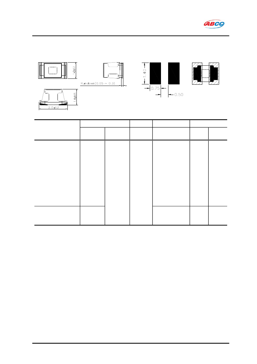
Shape & Dimensions / Recommended Solder Land Pattern
| LPS181214T-100M | LPS181214 | LPS181214T-150M | LPS181214T-1R0M | LPS181214T-1R5M | LPS181214T-220M | LPS181214T-2R2M | LPS181214T-3R3M | LPS181214T-4R7M | LPS181214T-6R8M | |
|---|---|---|---|---|---|---|---|---|---|---|
| Description | Shape & Dimensions / Recommended Solder Land Pattern | Shape & Dimensions / Recommended Solder Land Pattern | Shape & Dimensions / Recommended Solder Land Pattern | Shape & Dimensions / Recommended Solder Land Pattern | Shape & Dimensions / Recommended Solder Land Pattern | Shape & Dimensions / Recommended Solder Land Pattern | Shape & Dimensions / Recommended Solder Land Pattern | Shape & Dimensions / Recommended Solder Land Pattern | Shape & Dimensions / Recommended Solder Land Pattern | Shape & Dimensions / Recommended Solder Land Pattern |
 京公网安备 11010802033920号


