14 Pin DIL Triple TTL Compatible Active Delay Lines
DELAY TIME
±5% or 2 nS†
5
6
7
8
9
10
11
12
13
14
15
16
17
18
PART
NUMBER
EPA189-5
EPA198-6
EPA189-7
EPA189-8
EPA189-9
EPA18910
EPA189-11
EPA189-12
EPA189-13
EPA189-14
EPA189-15
EPA189-16
EPA189-17
EPA189-18
DELAY TIME
±5 or 2 nS†
19
20
21
22
23
24
25
30
35
40
45
50
55
60
PART
NUMBER
EPA189-19
EPA189-20
EPA189-21
EPA189-22
EPA189-23
EPA189-24
EPA189-25
EPA189-30
EPA189-35
EPA189-40
EPA189-45
EPA189-50
EPA189-55
EPA189-60
DELAY TIME
±5% or 2 nS†
65
70
75
80
85
90
95
100
125
150
175
200
225
250
PART
NUMBER
EPA189-65
EPA189-70
EPA189-75
EPA189-80
EPA189-85
EPA189-90
EPA189-95
EPA189-100
EPA189-125
EPA189-150
EPA189-175
EPA189-200
EPA189-225
EPA189-250
†
Whichever is greater. Delay Times referenced from input to leading edges at 25°C, 5.0V, with no load.
DC Electrical Characteristics
Parameter
VOH
VOL
VIK
IIH
IIL
IOS
ICCH
ICCL
TRO
NH
NL
High-Level Output Voltage
Low-Level Output Voltage
Input Clamp Voltage
High-Level Input Current
Low-Level Input Current
Short Circuit Output Current
High-Level Supply Current
Low-Level Supply Current
Output Rise Time
Fanout High-Level Output
Fanout Low-Level Output
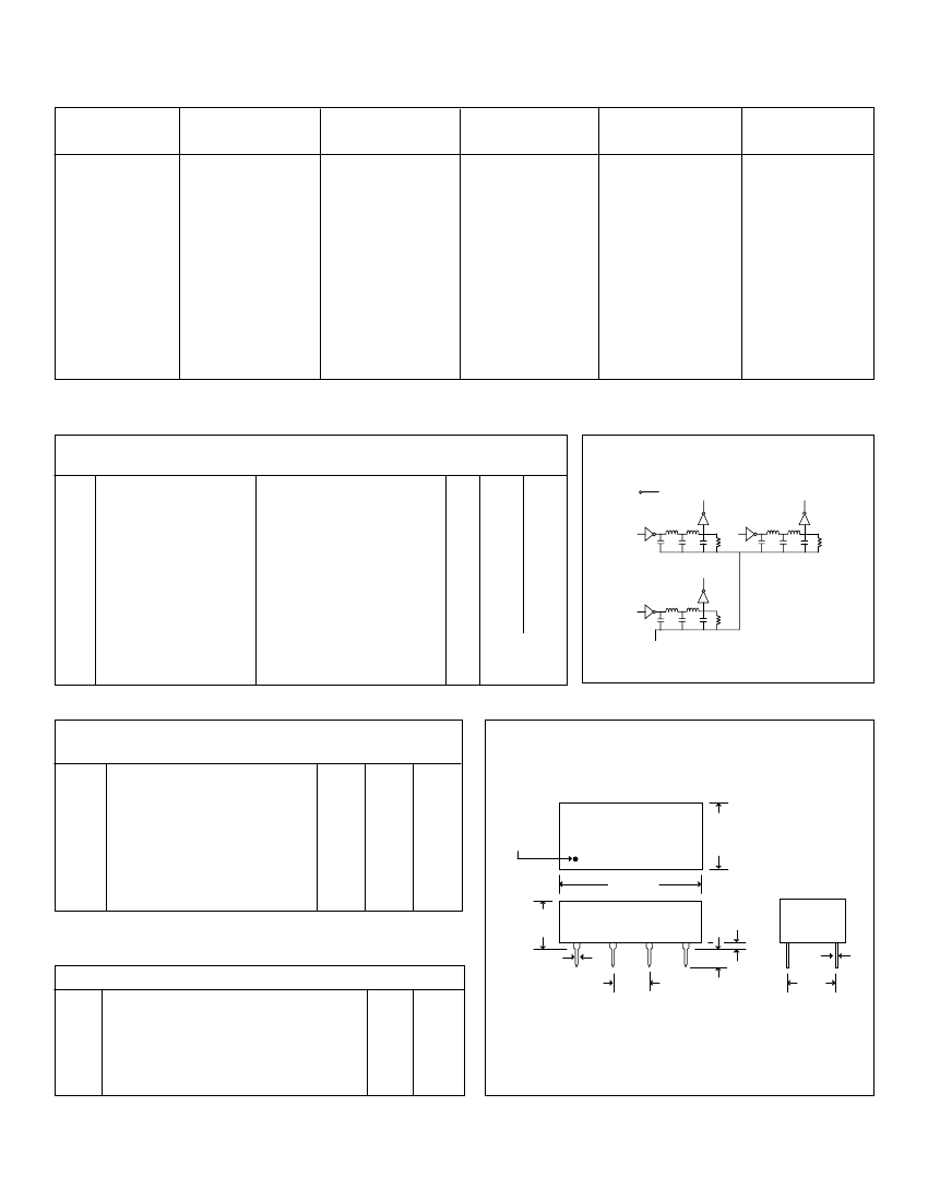
Schematic
Test Conditions
Min Max Unit
2.7
0.5
-1.2V
50
1.0
-2
-100
V
V
V
µA
mA
mA
mA
14
VCC
12
10
VCC = min. VIL = max. I OH = max
VCC = min. VIH = min. I OL= max
VCC = min. II = II K
VCC = max. VIN = 2.7V
VCC = max. VIN = 5.25V
VCC = max. VIN = 0.5V
VCC = max. VOUT = 0.
(One output at a time)
VCC = max. VIN = OPEN
VCC = max. VIN = 0
Td
≤
500 nS (0.75 to 2.4 Volts)
VCC = max. VOH = 2.7V
VCC = max. VOL = 0.5V
1
8
3
-40
115
mA
115
mA
4
nS
20 TTL LOAD
10 TTL LOAD
5
7 GROUND
Recommended
Operating Conditions
VCC
VIH
VIL
IIK
IOH
IOL
PW*
d*
TA
Supply Voltage
High-Level Input Voltage
Low-Level Input Voltage
Input Clamp Current
High-Level Output Current
Low-Level Output Current
Pulse Width of Total Delay
Duty Cycle
Operating Free-Air Temperature
Package Dimensions
Min
4.75
2.0
Max
5.25
0.8
-18
-1.0
20
Unit
V
V
V
mA
mA
mA
%
%
°C
White Dot
Pin#1
PCA
EPA189-5
Date Code
.800 Max.
.400
Max.
40
0
40
+70
*These two values are inter-dependent.
.275
Max.
.018
.020
Typ.
.010
.300
.150 Typ.
.200
Input Pulse Test Conditions @ 25° C
EIN
PW
TRI
PRR
VCC
Pulse Input Voltage
Pulse Width % of Total Delay
Pulse Rise Time (0.75 - 2.4 Volts)
Pulse Repetition Rate @ Td
≤
200 nS
Pulse Repetition Rate @ Td > 200 nS
Supply Voltage
3.2
110
2.0
1.0
100
5.0
Unit
Volts
%
nS
MHz
KHz
Volts
 京公网安备 11010802033920号


