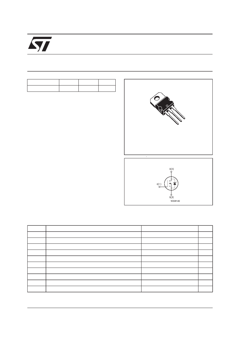
30 A, 50 V, 0.04 ohm, N-CHANNEL, Si, POWER, MOSFET, TO-220AB
| Parameter Name | Attribute value |
| Is it Rohs certified? | incompatible |
| Maker | STMicroelectronics |
| Parts packaging code | TO-220AB |
| package instruction | FLANGE MOUNT, R-PSFM-T3 |
| Contacts | 3 |
| Reach Compliance Code | _compli |
| ECCN code | EAR99 |
| Avalanche Energy Efficiency Rating (Eas) | 200 mJ |
| Configuration | SINGLE WITH BUILT-IN DIODE |
| Minimum drain-source breakdown voltage | 50 V |
| Maximum drain current (Abs) (ID) | 30 A |
| Maximum drain current (ID) | 33 A |
| Maximum drain-source on-resistance | 0.04 Ω |
| FET technology | METAL-OXIDE SEMICONDUCTOR |
| Maximum feedback capacitance (Crss) | 250 pF |
| JEDEC-95 code | TO-220AB |
| JESD-30 code | R-PSFM-T3 |
| JESD-609 code | e0 |
| Number of components | 1 |
| Number of terminals | 3 |
| Operating mode | ENHANCEMENT MODE |
| Maximum operating temperature | 175 °C |
| Package body material | PLASTIC/EPOXY |
| Package shape | RECTANGULAR |
| Package form | FLANGE MOUNT |
| Peak Reflow Temperature (Celsius) | NOT SPECIFIED |
| Polarity/channel type | N-CHANNEL |
| Maximum power consumption environment | 120 W |
| Maximum power dissipation(Abs) | 75 W |
| Maximum pulsed drain current (IDM) | 134 A |
| Certification status | Not Qualified |
| surface mount | NO |
| Terminal surface | Tin/Lead (Sn/Pb) |
| Terminal form | THROUGH-HOLE |
| Terminal location | SINGLE |
| Maximum time at peak reflow temperature | NOT SPECIFIED |
| transistor applications | SWITCHING |
| Transistor component materials | SILICON |
| Maximum off time (toff) | 400 ns |
| Maximum opening time (tons) | 165 ns |
 京公网安备 11010802033920号


