
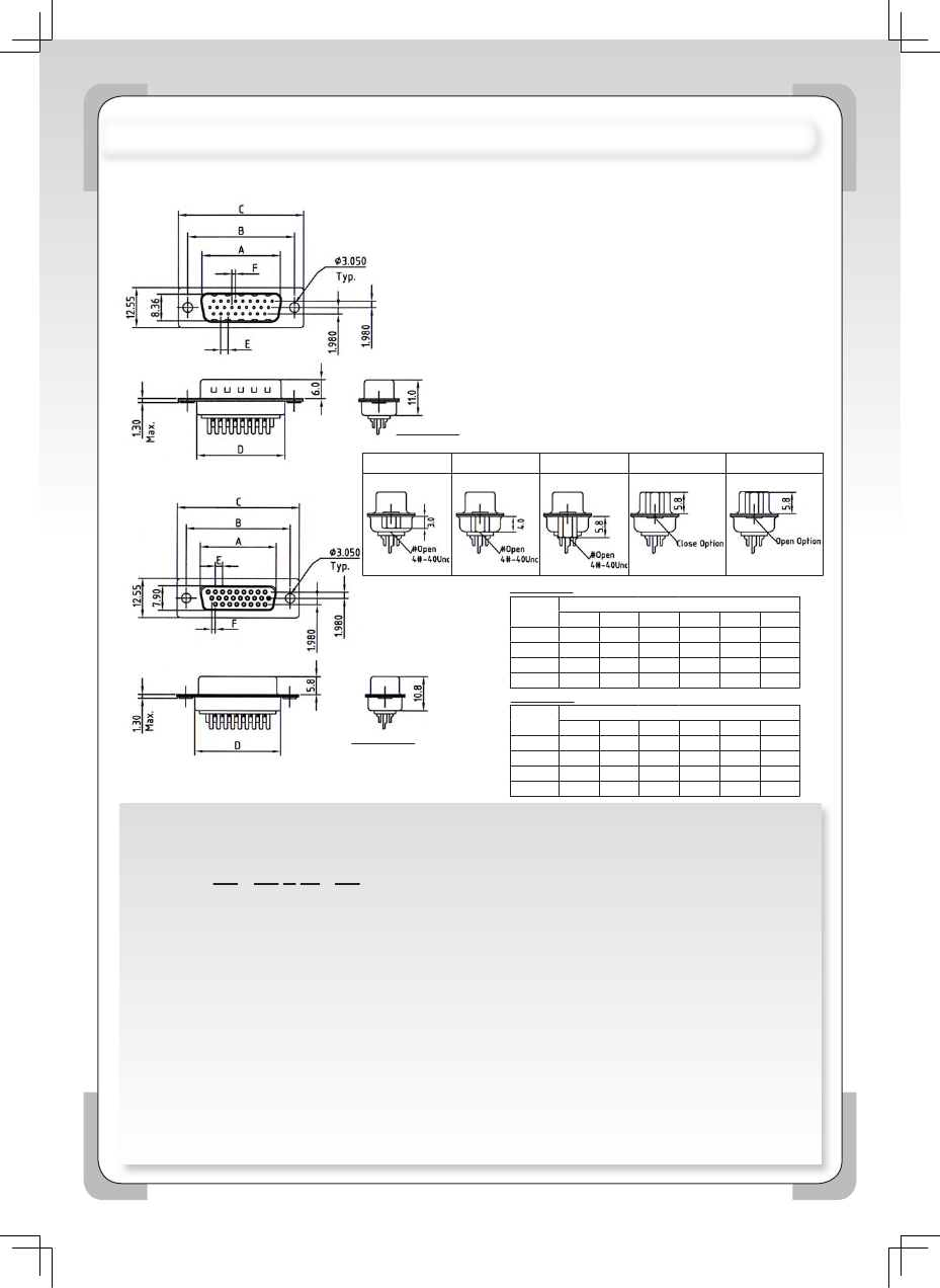
D Type Connector, 62 Contact(s), Male, Solder Lug Terminal, Locking, Receptacle
| Parameter Name | Attribute value |
| Is it Rohs certified? | conform to |
| Objectid | 307113941 |
| Reach Compliance Code | compliant |
| ECCN code | EAR99 |
| body width | 0.494 inch |
| body length | 2.728 inch |
| Body/casing type | RECEPTACLE |
| Contactor design | PREASSEM CONN |
| Contact to complete cooperation | AU ON NI |
| Contact point gender | MALE |
| Contact material | BRASS |
| contact mode | STAGGERED |
| Contact resistance | 25 mΩ |
| Contact style | RND PIN-SKT |
| Dielectric withstand voltage | 1000VAC V |
| Insulation resistance | 1000000000 Ω |
| Insulator color | WHITE |
| insulator material | POLYBUTYLENE TEREPHTHALATE |
| Installation option 1 | LOCKING |
| Installation type | PANEL |
| Number of rows loaded | 3 |
| Maximum operating temperature | 105 °C |
| Minimum operating temperature | -55 °C |
| Options | GENERAL PURPOSE |
| Rated current (signal) | 5 A |
| Guideline | UL |
| reliability | COMMERCIAL |
| Shell surface | TIN |
| Shell material | BRASS |
| Termination type | SOLDER LUG |
| Total number of contacts | 62 |
 京公网安备 11010802033920号


