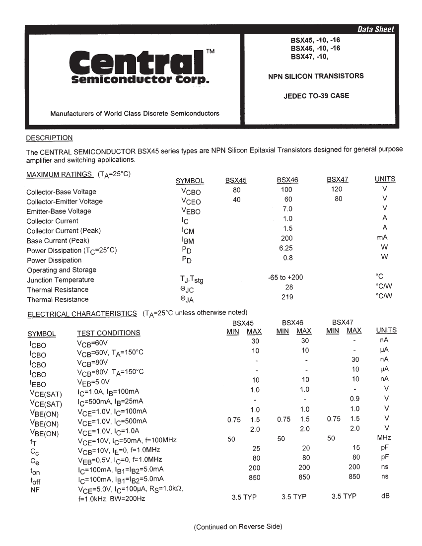
Small Signal Bipolar Transistor, 1A I(C), 80V V(BR)CEO, 1-Element, NPN, Silicon, TO-39, TO-39, 3 PIN
| Parameter Name | Attribute value |
| Is it lead-free? | Contains lead |
| Is it Rohs certified? | incompatible |
| Maker | Central Semiconductor |
| Parts packaging code | TO-39 |
| package instruction | TO-39, 3 PIN |
| Contacts | 3 |
| Reach Compliance Code | unknown |
| ECCN code | EAR99 |
| Maximum collector current (IC) | 1 A |
| Collector-based maximum capacity | 15 pF |
| Collector-emitter maximum voltage | 80 V |
| Configuration | SINGLE |
| Minimum DC current gain (hFE) | 25 |
| JEDEC-95 code | TO-39 |
| JESD-30 code | O-MBCY-W3 |
| JESD-609 code | e0 |
| Number of components | 1 |
| Number of terminals | 3 |
| Maximum operating temperature | 200 °C |
| Minimum operating temperature | -65 °C |
| Package body material | METAL |
| Package shape | ROUND |
| Package form | CYLINDRICAL |
| Peak Reflow Temperature (Celsius) | NOT SPECIFIED |
| Polarity/channel type | NPN |
| Maximum power consumption environment | 0.8 W |
| Maximum power dissipation(Abs) | 6.25 W |
| Certification status | Not Qualified |
| surface mount | NO |
| Terminal surface | Tin/Lead (Sn/Pb) |
| Terminal form | WIRE |
| Terminal location | BOTTOM |
| Maximum time at peak reflow temperature | NOT SPECIFIED |
| transistor applications | SWITCHING |
| Transistor component materials | SILICON |
| Nominal transition frequency (fT) | 50 MHz |
| Maximum off time (toff) | 850 ns |
| Maximum opening time (tons) | 200 ns |
| VCEsat-Max | 0.9 V |
| Base Number Matches | 1 |
| BSX47-10 | BSX46-10 | BSX46-16 | BSX45-16 | BSX45-10 | |
|---|---|---|---|---|---|
| Description | Small Signal Bipolar Transistor, 1A I(C), 80V V(BR)CEO, 1-Element, NPN, Silicon, TO-39, TO-39, 3 PIN | Small Signal Bipolar Transistor, 1A I(C), 60V V(BR)CEO, 1-Element, NPN, Silicon, TO-39, TO-39, 3 PIN | Small Signal Bipolar Transistor, 1A I(C), 60V V(BR)CEO, 1-Element, NPN, Silicon, TO-39, TO-39, 3 PIN | Small Signal Bipolar Transistor, 1A I(C), 40V V(BR)CEO, 1-Element, NPN, Silicon, TO-39, TO-39, 3 PIN | Small Signal Bipolar Transistor, 1A I(C), 40V V(BR)CEO, 1-Element, NPN, Silicon, TO-39, TO-39, 3 PIN |
| Is it lead-free? | Contains lead | Contains lead | Contains lead | Contains lead | Contains lead |
| Is it Rohs certified? | incompatible | incompatible | incompatible | incompatible | incompatible |
| Maker | Central Semiconductor | Central Semiconductor | Central Semiconductor | Central Semiconductor | Central Semiconductor |
| Parts packaging code | TO-39 | TO-39 | TO-39 | TO-39 | TO-39 |
| package instruction | TO-39, 3 PIN | TO-39, 3 PIN | CYLINDRICAL, O-MBCY-W3 | TO-39, 3 PIN | TO-39, 3 PIN |
| Contacts | 3 | 3 | 3 | 3 | 3 |
| Reach Compliance Code | unknown | unknown | not_compliant | unknown | unknown |
| ECCN code | EAR99 | EAR99 | EAR99 | EAR99 | EAR99 |
| Maximum collector current (IC) | 1 A | 1 A | 1 A | 1 A | 1 A |
| Collector-emitter maximum voltage | 80 V | 60 V | 60 V | 40 V | 40 V |
| Configuration | SINGLE | SINGLE | SINGLE | SINGLE | SINGLE |
| Minimum DC current gain (hFE) | 25 | 25 | 35 | 35 | 25 |
| JEDEC-95 code | TO-39 | TO-39 | TO-39 | TO-39 | TO-39 |
| JESD-30 code | O-MBCY-W3 | O-MBCY-W3 | O-MBCY-W3 | O-MBCY-W3 | O-MBCY-W3 |
| JESD-609 code | e0 | e0 | e0 | e0 | e0 |
| Number of components | 1 | 1 | 1 | 1 | 1 |
| Number of terminals | 3 | 3 | 3 | 3 | 3 |
| Maximum operating temperature | 200 °C | 200 °C | 200 °C | 200 °C | 200 °C |
| Package body material | METAL | METAL | METAL | METAL | METAL |
| Package shape | ROUND | ROUND | ROUND | ROUND | ROUND |
| Package form | CYLINDRICAL | CYLINDRICAL | CYLINDRICAL | CYLINDRICAL | CYLINDRICAL |
| Peak Reflow Temperature (Celsius) | NOT SPECIFIED | NOT SPECIFIED | NOT SPECIFIED | NOT SPECIFIED | NOT SPECIFIED |
| Polarity/channel type | NPN | NPN | NPN | NPN | NPN |
| Maximum power dissipation(Abs) | 6.25 W | 6.25 W | 5 W | 6.25 W | 6.25 W |
| Certification status | Not Qualified | Not Qualified | Not Qualified | Not Qualified | Not Qualified |
| surface mount | NO | NO | NO | NO | NO |
| Terminal surface | Tin/Lead (Sn/Pb) | Tin/Lead (Sn/Pb) | Tin/Lead (Sn/Pb) | Tin/Lead (Sn/Pb) | Tin/Lead (Sn/Pb) |
| Terminal form | WIRE | WIRE | WIRE | WIRE | WIRE |
| Terminal location | BOTTOM | BOTTOM | BOTTOM | BOTTOM | BOTTOM |
| Maximum time at peak reflow temperature | NOT SPECIFIED | NOT SPECIFIED | NOT SPECIFIED | NOT SPECIFIED | NOT SPECIFIED |
| transistor applications | SWITCHING | SWITCHING | SWITCHING | SWITCHING | SWITCHING |
| Transistor component materials | SILICON | SILICON | SILICON | SILICON | SILICON |
| Nominal transition frequency (fT) | 50 MHz | 50 MHz | 50 MHz | 50 MHz | 50 MHz |
| Maximum off time (toff) | 850 ns | 850 ns | 850 ns | 850 ns | 850 ns |
| Maximum opening time (tons) | 200 ns | 200 ns | 200 ns | 200 ns | 200 ns |
| Collector-based maximum capacity | 15 pF | 20 pF | - | 25 pF | 25 pF |
| Minimum operating temperature | -65 °C | -65 °C | - | -65 °C | -65 °C |
| Maximum power consumption environment | 0.8 W | 0.8 W | - | 0.8 W | 0.8 W |
| VCEsat-Max | 0.9 V | 1 V | - | 1 V | 1 V |
| Base Number Matches | 1 | 1 | 1 | - | - |
 京公网安备 11010802033920号


