5962F0151001QXC amplifier basic information:
5962F0151001QXC is a COMPARATOR. Commonly used packaging methods are DFP, FL20,.3
5962F0151001QXC amplifier core information:
The minimum operating temperature of 5962F0151001QXC is -55 °C and the maximum operating temperature is 125 °C. Maximum bias current at 25°C: 1 µA Maximum average bias current is 1 µA
When it comes to an amplifier's sensitivity, nothing is better than its nominal response time. 5962F0151001QXC takes only 7000 ns to respond. The maximum slew rate of the 5962F0151001QXC given by the manufacturer is 3.5 mA.
The nominal supply voltage of the 5962F0151001QXC is 9 V. The power supply range is: 9/30 V. The input offset voltage of the 5962F0151001QXC is 5000 µV (Input offset voltage: the compensation voltage between the two input terminals required to make the op amp output terminal 0V (or close to 0V).) The nominal supply voltage of the 5962F0151001QXC is 9 V.
Related dimensions of 5962F0151001QXC:
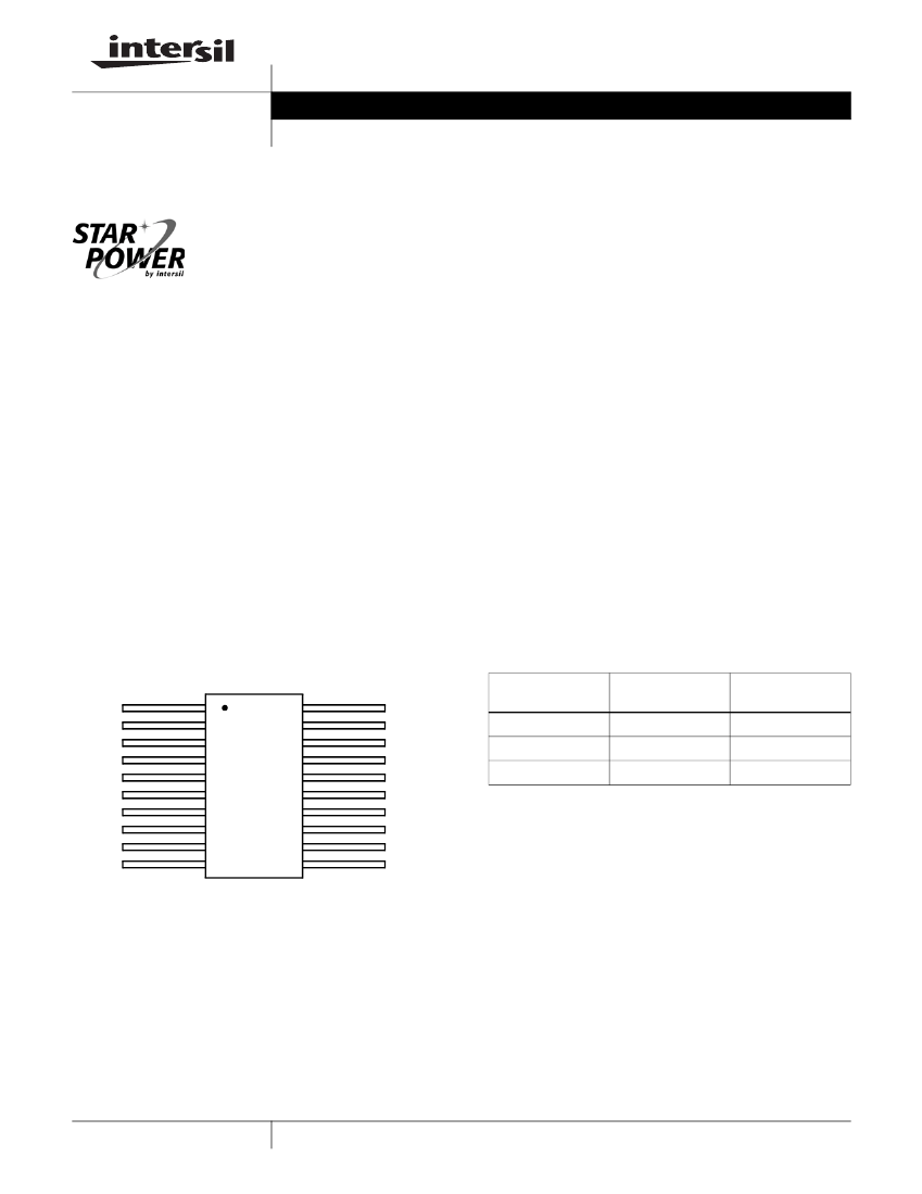
5962F0151001QXC has 20 terminals. Its terminal position type is: DUAL. Terminal pitch is 1.27 mm. Total pins: 20
5962F0151001QXC amplifier additional information:
Its temperature grade is: MILITARY. The corresponding JESD-30 code is: R-CDFP-F20. The corresponding JESD-609 code is: e4. The packaging code of 5962F0151001QXC is: DFP. The materials used in the 5962F0151001QXC package are mostly CERAMIC, METAL-SEALED COFIRED.
The package shape is RECTANGULAR. The 5962F0151001QXC package pin format is: FLATPACK. Its terminal form is: FLAT. The maximum seat height is 2.92 mm.
5962F0151001QXC amplifier basic information:
5962F0151001QXC is a COMPARATOR. Commonly used packaging methods are DFP, FL20,.3
5962F0151001QXC amplifier core information:
The minimum operating temperature of 5962F0151001QXC is -55 °C and the maximum operating temperature is 125 °C. Maximum bias current at 25°C: 1 µA Maximum average bias current is 1 µA
When it comes to an amplifier's sensitivity, nothing is better than its nominal response time. 5962F0151001QXC takes only 7000 ns to respond. The maximum slew rate of the 5962F0151001QXC given by the manufacturer is 3.5 mA.
The nominal supply voltage of the 5962F0151001QXC is 9 V. The power supply range is: 9/30 V. The input offset voltage of the 5962F0151001QXC is 5000 µV (Input offset voltage: the compensation voltage between the two input terminals required to make the op amp output terminal 0V (or close to 0V).) The nominal supply voltage of the 5962F0151001QXC is 9 V.
Related dimensions of 5962F0151001QXC:
5962F0151001QXC has 20 terminals. Its terminal position type is: DUAL. Terminal pitch is 1.27 mm. Total pins: 20
5962F0151001QXC amplifier additional information:
Its temperature grade is: MILITARY. The corresponding JESD-30 code is: R-CDFP-F20. The corresponding JESD-609 code is: e4. The packaging code of 5962F0151001QXC is: DFP. The materials used in the 5962F0151001QXC package are mostly CERAMIC, METAL-SEALED COFIRED.
The package shape is RECTANGULAR. The 5962F0151001QXC package pin format is: FLATPACK. Its terminal form is: FLAT. The maximum seat height is 2.92 mm.
| Parameter Name | Attribute value |
| Maker | Renesas Electronics Corporation |
| Parts packaging code | DFP |
| package instruction | DFP, FL20,.3 |
| Contacts | 20 |
| Reach Compliance Code | compliant |
| ECCN code | EAR99 |
| Amplifier type | COMPARATOR |
| Maximum average bias current (IIB) | 1 µA |
| Maximum bias current (IIB) at 25C | 1 µA |
| Maximum input offset voltage | 5000 µV |
| JESD-30 code | R-CDFP-F20 |
| JESD-609 code | e4 |
| Number of functions | 4 |
| Number of terminals | 20 |
| Maximum operating temperature | 125 °C |
| Minimum operating temperature | -55 °C |
| Output type | OPEN-COLLECTOR |
| Package body material | CERAMIC, METAL-SEALED COFIRED |
| encapsulated code | DFP |
| Encapsulate equivalent code | FL20,.3 |
| Package shape | RECTANGULAR |
| Package form | FLATPACK |
| power supply | 9/30 V |
| Certification status | Not Qualified |
| Nominal response time | 7000 ns |
| Filter level | MIL-PRF-38535 Class Q |
| Maximum seat height | 2.92 mm |
| Maximum slew rate | 3.5 mA |
| Supply voltage upper limit | 33 V |
| Nominal supply voltage (Vsup) | 9 V |
| surface mount | YES |
| technology | BIPOLAR |
| Temperature level | MILITARY |
| Terminal surface | GOLD |
| Terminal form | FLAT |
| Terminal pitch | 1.27 mm |
| Terminal location | DUAL |
| total dose | 300k Rad(Si) V |
| width | 6.92 mm |
| Base Number Matches | 1 |
| 5962F0151001QXC | 5962F0151001VXC | |
|---|---|---|
| Description | QUAD COMPARATOR, 5000uV OFFSET-MAX, CDFP20, CERAMIC, DFP-20 | QUAD COMPARATOR, 5000uV OFFSET-MAX, CDFP20, CERAMIC, DFP-20 |
| Maker | Renesas Electronics Corporation | Renesas Electronics Corporation |
| Parts packaging code | DFP | DFP |
| package instruction | DFP, FL20,.3 | DFP, FL20,.3 |
| Contacts | 20 | 20 |
| Reach Compliance Code | compliant | compliant |
| ECCN code | EAR99 | EAR99 |
| Amplifier type | COMPARATOR | COMPARATOR |
| Maximum average bias current (IIB) | 1 µA | 1 µA |
| Maximum bias current (IIB) at 25C | 1 µA | 1 µA |
| Maximum input offset voltage | 5000 µV | 5000 µV |
| JESD-30 code | R-CDFP-F20 | R-CDFP-F20 |
| JESD-609 code | e4 | e4 |
| Number of functions | 4 | 4 |
| Number of terminals | 20 | 20 |
| Maximum operating temperature | 125 °C | 125 °C |
| Minimum operating temperature | -55 °C | -55 °C |
| Output type | OPEN-COLLECTOR | OPEN-COLLECTOR |
| Package body material | CERAMIC, METAL-SEALED COFIRED | CERAMIC, METAL-SEALED COFIRED |
| encapsulated code | DFP | DFP |
| Encapsulate equivalent code | FL20,.3 | FL20,.3 |
| Package shape | RECTANGULAR | RECTANGULAR |
| Package form | FLATPACK | FLATPACK |
| power supply | 9/30 V | 9/30 V |
| Certification status | Not Qualified | Not Qualified |
| Nominal response time | 7000 ns | 7000 ns |
| Filter level | MIL-PRF-38535 Class Q | MIL-PRF-38535 Class V |
| Maximum seat height | 2.92 mm | 2.92 mm |
| Maximum slew rate | 3.5 mA | 3.5 mA |
| Supply voltage upper limit | 33 V | 33 V |
| Nominal supply voltage (Vsup) | 9 V | 9 V |
| surface mount | YES | YES |
| technology | BIPOLAR | BIPOLAR |
| Temperature level | MILITARY | MILITARY |
| Terminal surface | GOLD | GOLD |
| Terminal form | FLAT | FLAT |
| Terminal pitch | 1.27 mm | 1.27 mm |
| Terminal location | DUAL | DUAL |
| total dose | 300k Rad(Si) V | 300k Rad(Si) V |
| width | 6.92 mm | 6.92 mm |
 京公网安备 11010802033920号


