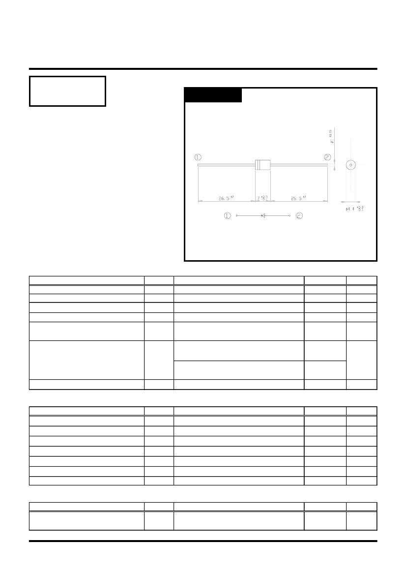
EEWORLDEEWORLDEEWORLD

Part Number

Search

K1V10

Description
sidac
CategoryAnalog mixed-signal IC    Trigger device   
File Size410KB,10 Pages
ManufacturerSHINDENGEN
Websitehttps://www.shindengen.com
Environmental Compliance
Download Datasheet Parametric View All

K1V10 Online Shopping

Suppliers Part Number Price MOQ In stock  
K1V10 - - View Buy Now

K1V10 Overview

sidac

K1V10 Parametric

Parameter NameAttribute value
Is it Rohs certified?conform to
MakerSHINDENGEN
Parts packaging codeAXIAL
package instructionLONG FORM, O-XALF-W2
Contacts2
Manufacturer packaging codeAX10
Reach Compliance Codeunknown
ECCN codeEAR99
Maximum breakover voltage113 V
Minimum breakover voltage95 V
Shell connectionISOLATED
ConfigurationSINGLE
Nominal holding current50 mA
JESD-30 codeO-XALF-W2
Humidity sensitivity level2
On-state non-repetitive peak current20 A
Number of components1
Number of terminals2
Maximum operating temperature125 °C
Minimum operating temperature-40 °C
Package body materialUNSPECIFIED
Package shapeROUND
Package formLONG FORM
Certification statusNot Qualified
Repeated peak reverse voltage90 V
surface mountNO
Terminal formWIRE
Terminal locationAXIAL
Trigger device typeSIDAC
SHINDENGEN
Sidac
K1V10
OUTLINE DIMENSIONS
Case : AX10
(Unit : mm)
RATINGS
●Absolute
Maximum Ratings
Item
Storage Temperature
Operating Junction Temperature
Maximum Off-state Voltage
RMS On-state Current
Surge On-state Current
Symbol
Tstg
Tj
V
DRM
I
T
Conditions
Tl =
112℃,
50Hz sine wave (θ =
180°)
Tj = 25℃, 50Hz sine wave (θ =
180°),
non-repetitive
1-cycle
peak value
Ta =25
℃,
pulse width t
o
=
10 μs,
sine wave,
repetitive peak value
f =
1
kHz
Ta =25
℃,
pulse width t
o
=
10 μs,
sine wave,
repetitive peak value
f = 60 Hz
I
TSM
Ratings
-40½125
125
90
1
20
25
Unit
V
A
A
Pulse On-state Current
I
TRM
A
80
80
Ratings
95½113
Max
10
Max 0.5
TYP 50
Max
1.5
Min 0.1
Max
15
Standard
1.2
A/μs
Unit
V
μA
mA
mA
V
℃/W
Unit
A
Critical Rate of Rise of On-state Current
di
T
/dt
●Electrical
Characteristics (Tl=25℃)
Item
Symbol
Breakover Voltage
V
BO
Off-state Current
I
DRM
Breakover Current
I
BO
Holding Current
I
H
On-state Voltage
V
T
Switching Resistance
R
S
Thermal Resistance
θjl
●Standard
Design with P.C.B.
Item
RMS On-state Current
Conditions
I
B
= 0, 50Hz sine wave
V
D
= V
DRM
I
T
=
1A
Junction to lead
Conditions
Symbol
Assembled in P.C.B., Ta = 25℃,
I
T
soldering land 3mmφ
Copyright & Copy;2000 Shindengen Electric Mfg.Co.Ltd

EEWorld
subscription
account

EEWorld
service
account

Automotive
development
circle

Robot
development
community

Index Files: 1732  406  2186  1004  218  35  9  45  21  5 
Datasheet   0 1 2 3 4 5 6 7 8 9 A B C D E F G H I J K L M N O P Q R S T U V W X Y Z
Room 1530, 15th Floor, Building B, No. 18 Zhongguancun Street, Haidian District, Beijing Telephone: (010) 82350740 Postal Code: 100190
Copyright © 2005-2026 EEWORLD.com.cn, Inc. All rights reserved 京ICP证060456号 京ICP备10001474号-1 电信业务审批[2006]字第258号函 京公网安备 11010802033920号