**2. Power module**
  **3. Display interface**
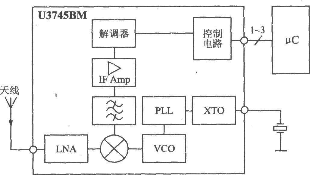
  **4. Buttons, headphones and other modules**
  ![image.png]
  **2. PCB design**
  ![image.png]
  ![image .png]
  ![image.png]
  ![Front.jpg]
  ![Back.jpg]
  The final product does not purchase pin sockets, and the battery power cord is directly welded to the board.
  ![image.png]
  Pay extra attention to the following two points
  ![image.png]
  (2) Lcd_PushStart needs to change the offset is 0, otherwise the screen will not be displayed in full screen
 ![image.png]
  ![image.png]
  The final effect
  ![WeChat picture_20230521160113.jpg]

All reference designs on this site are sourced from major semiconductor manufacturers or collected online for learning and research. The copyright belongs to the semiconductor manufacturer or the original author. If you believe that the reference design of this site infringes upon your relevant rights and interests, please send us a rights notice. As a neutral platform service provider, we will take measures to delete the relevant content in accordance with relevant laws after receiving the relevant notice from the rights holder. Please send relevant notifications to email: bbs_service@eeworld.com.cn.
It is your responsibility to test the circuit yourself and determine its suitability for you. EEWorld will not be liable for direct, indirect, special, incidental, consequential or punitive damages arising from any cause or anything connected to any reference design used.
Supported by EEWorld Datasheet
EEWorld
subscription
account

EEWorld
service
account

Automotive
development
community

Robot
development
community

About Us Customer Service Contact Information Datasheet Sitemap LatestNews


Room 1530, 15th Floor, Building B,
No.18 Zhongguancun Street,
Haidian District,
Beijing, Postal Code: 100190
China
Telephone: 008610 8235 0740
 京公网安备 11010802033920号

 MA-151-020-335