I actively responded to and participated in my first systematic electronic circuit practice – the #LCSC Digital Oscilloscope Training Camp.
I attended the oscilloscope training camp organized by JLCSC, independently watching and learning from the official videos and web learning materials. Step by step, I diligently learned and built a digital oscilloscope, which greatly helped my comprehensive electronic circuit skills. This digital oscilloscope project included the design and development of microcontroller circuits, calculation of signal conditioning circuits, design of human-computer interaction, and design of the enclosure model. It integrated knowledge of analog circuits, microcontroller design, circuit and PCB design, and enclosure design. Suitable for most beginners, I highly recommend everyone try building their first digital oscilloscope. This project has the following characteristics:
the core board uses the domestic GD32 as the main controller, and the minimum system development board GD32E230C8T6 released by JLCSC is used;
the project is highly comprehensive and practical, and can be used as a desktop instrument after completion;
the project has abundant learning materials, including circuit design tutorials, PCB design, and Keil code programming.
I. Main Controller GD32E230C8T6

II. Power Supply and Negative Voltage
Circuit: The oscilloscope is powered in reverse via a TYPE-C interface or a TYPE-C or SWD interface connected to the core board. This section only discusses the power supply of the oscilloscope's main board.
This case uses a 2-pin, 2-element TYPE-C interface. Pin 1 is connected to the external positive VCC, and pin 2 is connected to GND. The external VCC is switched via a three-pin switch SW1: pins 1-2 are OFF, and pins 2-3 are ON. The obtained 5V VCC, after being processed by capacitor C1, first powers the negative voltage circuit of the XD7660, thus generating a negative voltage supply. A 1kΩ resistor is connected in series with an external LED for power indication. PS: The function of capacitor C1 here is DC blocking coupling, used to transmit AC signals and isolate DC, preventing mutual interference between DC potentials of the preceding and following stages, thereby more effectively eliminating distortion and making the square wave pattern more accurate.
XD7660: This circuit is purely for converting +5V to -5V to generate a negative voltage for pin 4 of the TL072IP chip, which is then used in the oscilloscope's data measurement. The circuit here is relatively simple. For further information, please refer to the LCSC tutorial video at the following address: http://bilibili.com/video/BV13x4y1k7mk/?spm_id_from=333.788&vd_source=2fafdf31a8203b41032c15579930bf64
(around 37 minutes).

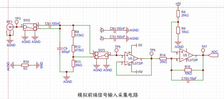
III. Analog Front-End Acquisition Circuit
TL072IP: This circuit handles the analog front-end acquisition and processing. The TL072 performs dual-channel processing on the acquired signals.
In the circuit, the leftmost part is the signal acquisition interface BNC, used to acquire the required data. The first switch, SW2, switches between DC/AC (DC signal/AC signal).
The acquired signal, if switched to AC, will first pass through C5 for DC blocking and AC passing, and then undergo frequency discrimination and filtering. After being divided by R8, R12, and R13, it will be selected by SW3 to enter the 072 chip for processing. The calculation formula is 20K/510K + 470K + 20K = 20/1000 = 1/50, which is equivalent to the input signal being attenuated by about 50 times for analysis. PS: The key function here is to protect the entire circuit. It is recommended to first switch SW2 to the attenuation range 2-3 for measurement. When the measured voltage value is low, you can switch to range 1-2 for further measurement. I've seen friends burn out their 072 chips, most likely because they were measured using range 1-2. Therefore, I strongly recommend prioritizing measurements using range 2-3 to protect the chips in the circuit, and also because measurements at range 2-3 are more accurate.
If the signal enters through the DC input of SW2 (1-2), it first passes through C9 to remove high-frequency signal noise, circuit coupling, and high-frequency filtering. Then, it is connected in series with resistors such as R13 and connected to SW3 before being connected to pin 3 of the 072 chip for processing. After processing, select 1-2 or 2-3 using SW3. Here, "ps" is crucial: "Ideal value: When switched to pin 1-2 of SW3, the measured voltage range is -80V to 250V; ideal value: When switched to pin 2-3 of SW3, the measured voltage range is -1.6V to 5V. Due to impedance, there may be a situation where the oscilloscope shows no waveform after switching SW3 to 2-3. This is related to the BNC probe used. Ideally, using a passive probe might avoid this situation. In daily use, a BNC to alligator probe is used, so the absence of waveform may be due to the measured voltage value exceeding the measurement range calculated by the oscilloscope's program design. Don't panic; you can measure voltages within other measurable ranges to determine if it's not a problem with this oscilloscope." This section is too long; please refer to the official tutorial video. This section
borrows from @Q1ngXun's circuit explanation. The following is a quote from @Q1ngXun's original explanation; if there is any infringement, please inform us and we will delete it immediately!
-------------------------------------------------@Q1ngXun's Original Explanation--------------------------------------------------------------
"4. In the TL072IP op-amp, section U5.2 acts as a voltage follower. Input pin 2 is connected to output pin 1. Considering the virtual short characteristic of the op-amp, V+=V-=Vout. Based on the virtual open circuit characteristic, the op-amp's input impedance is relatively large, so the forward input current is very small. The op-amp's output impedance is small, so the output current is very large. This indicates that the voltage follower here plays an impedance matching role.
5. In the TL072IP op-amp, section U5.1 acts as a proportional amplifier circuit, which can be divided into a non-inverting proportional amplifier circuit and an inverting proportional amplifier circuit, depending on the situation. Assuming the op-amp's positive input terminal is grounded, it forms an inverting proportional amplifier circuit; assuming the op-amp's inverting input terminal is grounded, it forms a non-inverting proportional amplifier circuit."
-------------------------------------------------@Q1ngXun's Original Explanation--------------------------------------------------------------
This circuit is the core circuit. For details, please refer to the LCSC tutorial video https://www.bilibili.com/video/BV13x4y1k7mk/?spm_id_from=333.788&vd_source=2fafdf31a8203b41032c15579930bf64.
Detailed instructions are available from around 5 minutes and 42 seconds!
IV. Comparator Frequency Measurement Circuit
LN393: Implements frequency detection, using the microcontroller's timer capture function to calculate the period of the input waveform.
Pin 8 is connected to a 3V3 circuit, and pin 2 is connected to the digital signal converted from the analog signal, which is provided to pin 1 to output the compared FREQ (frequency).
Pin 3 cooperates with the voltage drop from the 3V3 circuit via a 10KΩ resistor in series, which is then fed into pin 3. Another path, connected to a 510KΩ resistor in series, flows into pin 1 for data comparison.

V. Rotary Encoder and TFT Circuit
: TFT: 1.8-inch, 128 x 160 pixels, connects to the microcontroller via 8 pins. Used to display the acquired signal waveform and frequency information.
Rotary Encoder: Adjusts the horizontal range of the waveform display on the screen; buttons are used to pause/start the waveform.

VI. Button Control Circuit and LED Status
KEY1: PWM duty cycle.
KEY2: PWM output on/off.
KEY3: Adjusts the frequency waveform of the PWM output, rotating to display 1K/2K/4K.

LED2 and LED3 are connected to the C14 and C15 ports of the GD32 for control of whether they blink. These two LEDs are not enabled in the source code; to enable them, add the light-on code to the main function. The two LEDs, KEY1-KEY3, and EC11 are linked and will blink in response to the button and rotation.
VII. Completed Image

------------------------------------- Problems Encountered ------------------------------------
1. None.
Perhaps it's my innate passion for electronic circuits, but as a complete beginner, I managed to complete such a complex circuit on my first try. From drawing the schematic to generating the PCB, then prototyping the circuit board, soldering it, and flashing the program, I did it all in one go without encountering any problems. (This is probably due to the dedication of the video instructors and my own careful watching of every minute of the tutorial videos. I watched each episode three or five times, repeatedly reviewing the videos when I encountered problems I didn't understand, and repeatedly watching and pausing the videos when I couldn't draw the models or routing. Although this took up a lot of precious time with my family, I feel it was all worthwhile. This training camp has transformed me from a complete novice to someone who can now guide others in the group when they encounter problems. I also found the learning process very enjoyable and fulfilling. I not only learned knowledge but also made many good friends and met some experts. Due to space limitations, I won't name them all, but I would like to say "Thank you!" to all the friends who helped and guided me.)
---------------------------------------Summary---------------------------------------
As a complete beginner, this was my first systematic participation in the LCSC training camp. There may be shortcomings in the documentation, so please feel free to point them out. I hope to learn and improve together with everyone. I'm also grateful to the LCSC open-source platform for giving me this invaluable learning opportunity, from which I learned a lot of previously unknown knowledge. I especially thank Mr. Mo for his detailed explanations in the videos and tutorials, which enabled me, a complete beginner, to successfully replicate this digital oscilloscope on my first try. I'm incredibly excited and grateful.
Due to video limitations, the complete video is uploaded to Bilibili. Please feel free to offer your criticism and suggestions! The test video and the entire production and learning process are condensed into a video of about 6 minutes. The audio is in stereo; if you don't want to hear my rambling, just turn on the left channel; if you don't want to listen to music, just turn on the right channel! The viewing link is as follows:
https://www.bilibili.com/video/BV1rx421Q7D8/


 京公网安备 11010802033920号

 MI-P2XL-MYV


