Load transient response test of voltage regulator (3)
Source: InternetPublisher:张小哥 Keywords: Voltage regulator load transient response Updated: 2025/09/30
The role of capacitors in regulator response
This regulator uses capacitors at its input (C IN ) and output (C OUT ) to enhance its high-frequency response. Careful consideration should be given to the capacitor's dielectric, value, and placement, as they significantly affect the regulator's characteristics. C OUT dominates the regulator's dynamic response; C IN is much less important, as long as it does not fall below the regulator's dropout point. Figure 16 shows a typical regulator circuit, highlighting C OUT and its parasitics. Parasitic inductance and resistance limit the capacitor's effectiveness over frequency. The capacitor's dielectric and value significantly affect the load-step response. "Hidden" parasitic impedance buildup in the regulator's output traces can also affect regulation characteristics, although you can minimize parasitic effects through remote sensing and distributed capacitor bypassing.
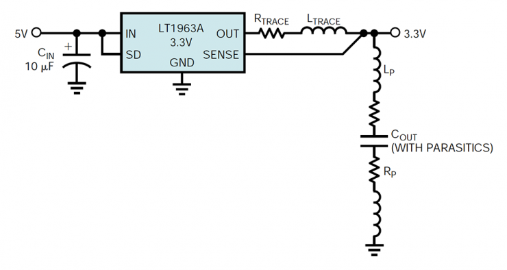
Figure 16. C OUT dominates the regulator's dynamic response; C IN is much less important. Parasitic inductance and resistance limit the capacitor's effectiveness over frequency. The capacitor's value and dielectric significantly affect the load-step response. Excessive trace impedance is also a factor.
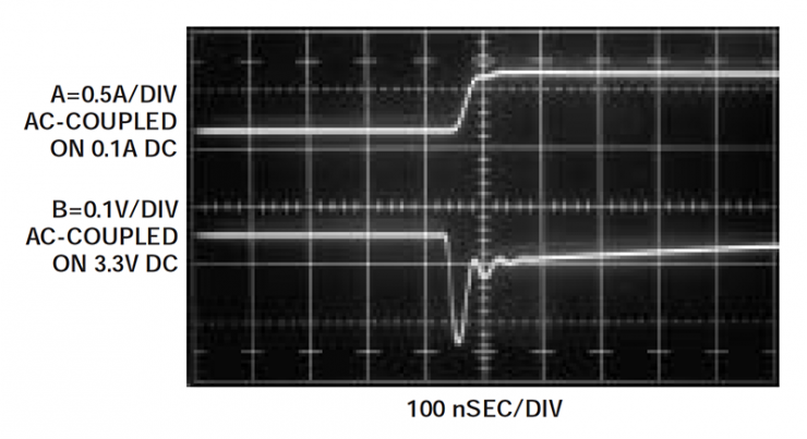
Figure 17 shows the response of the circuit in Figure 16 (Trace B) to a 0.5A load step biased at 0.1A DC (Trace A) with C IN = C OUT = 10 µF. The circuit uses low-loss capacitors, resulting in well-controlled output in Trace B. Figure 18 significantly expands the horizontal time scale to investigate high-frequency behavior. The regulator output deviation (Trace B) is smooth, with no abrupt discontinuities. Figure 19 runs the same test as Figure 17, using output capacitors claimed to be "equivalent" to those used in Figure 17.
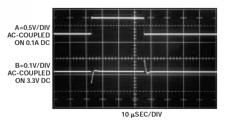
Figure 17. A step 0.5A load applied to the circuit of Figure 16 (Trace A) with C IN =C OUT =10 µF results in the regulator output of Trace B. The use of low-loss capacitors facilitates controlled output excursion.
The expanded horizontal scale in Figure 18 shows the smooth regulator output response of Trace B. Mismatched current and voltage probe delays cause a slight time offset.
The 10-FC OUT capacitor in Figure 19 and Figure 17, which are “equivalent” to the capacitors in Figure 17, show similar performance at 10 seconds/div.
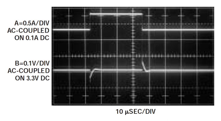
Expanding horizontally in Figure 20 shows that the “equivalent” capacitor produces twice the amplitude error of the capacitor in Figure 18. Unmatched probe delays can cause time skew between traces.
At 10 µsec/div, the oscilloscope photos look similar, but Figure 20 reveals a problem. This photo, taken at the same higher sweep speed as the one in Figure 18, shows that the "equivalent" capacitor has twice the amplitude error, higher frequency content, and higher resonance than the capacitor in Figure 18. (Always specify components based on observed performance, not what the salesperson says.) Figure 21 replaces C OUT with a lossy 10 µF unit. This capacitor allows a 400-mV offset (note the change in the vertical scale on Trace B), four times greater than in Figure 18. Conversely, Figure 22 increases C OUT to a low-loss 33 µF type, reducing the output response transient in Trace B by 40% compared to Figure 18. Figure 23 further adds a low-loss 330-µF capacitor, keeping the transient to within 20 mV: four times lower than the 10-µF value in Figure 18.
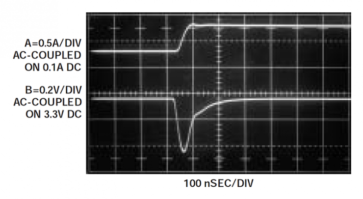
Figure 21 shows a 10-µF COUT with excessive losses, allowing for a 400-mV offset—four times that of Figure 18. The timing skew between the traces is due to probe mismatch.
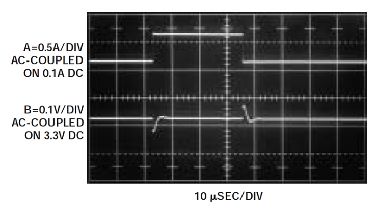
Figure 22. Replacing C OUT with a low-loss 33-µF cell produces an output response transient that is 40% smaller than that in Figure 17.
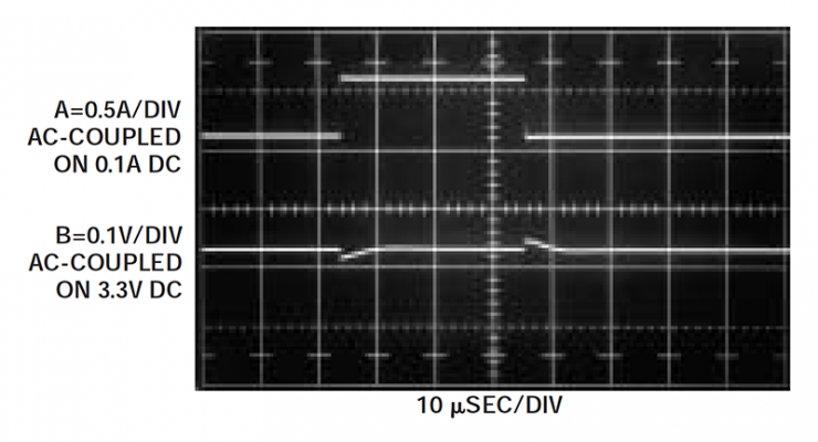
Figure 23. The low-loss, 330µF capacitor keeps the output response transient below 20mV—four times lower than the 10µF capacitor in Figure 17.
The lesson is clear: capacitor value and dielectric quality have a significant effect on transient load response. Try it before you specify!
Rise Time and Regulator Response
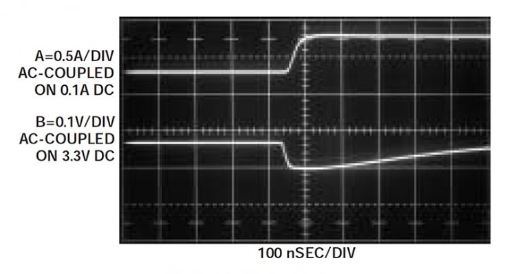
A closed-loop load transient generator also allows for studying the load transient rise time during high-speed regulation. Figure 24 shows the circuit of Figure 16 (C IN = C OUT = 10 µF) responding to a 0.5A, 100ns rise time step on a 0.1A DC load (Trace A). The response rolloff (Trace B) peaks at 75 mV and exhibits some distortion. Reducing the load step rise time of Trace A (Figure 25) nearly doubles the response error of Trace B, with the accompanying tracking distortion also increasing. This behavior indicates increased regulator error at higher frequencies.
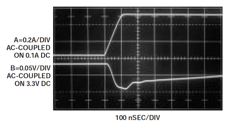
Figure 24 shows the regulator's output response (Trace B) to a 100 nanosecond rise time current step at COUT (Trace A) of 10 µF. The response decays to a peak of 75 mV.
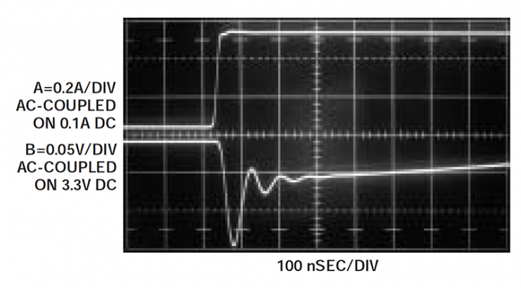
Figure 25 A faster rise time current step (Trace A) increases the response decay peak (Trace B) to 140 mV, indicating that regulation loss increases with frequency.
All regulators exhibit errors that increase with frequency—some more than others. Slow load transients can unfairly make a bad regulator look good. It is questionable if transient load testing does not indicate some response outside the regulator's bandwidth.
Intel's embedded memory regulator provides a good practical example illustrating the importance of a regulator's load-step performance. The memory requires a 1.8V supply, typically regulated down from 3V. While the current requirements are relatively modest, the supply tolerance is tight. Table 1 shows that only a 0.1V deviation from 1.8V is allowed, including all DC and dynamic errors. The LTC1844-1.8 regulator has an initial tolerance of 1.75% at 31.5mV, leaving only 68.5mV of dynamic error margin. Figure 26 shows the test circuit. The memory control line movement causes a 50mA load transient, necessitating careful capacitor selection. (The LTC1844-1.8's noise bypass pin works with an optional external capacitor to achieve low output noise. However, this application does not require it and should be left unconnected.) C IN is optional if the regulator is located close to the supply. If not, use a high-quality 1µF capacitor for C IN. C OUT is a low-loss, 1µF type. In all other respects, the circuit appears to be routine.
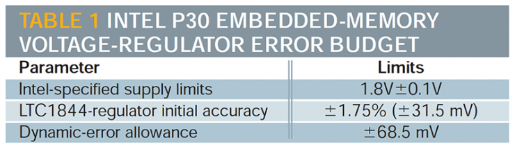
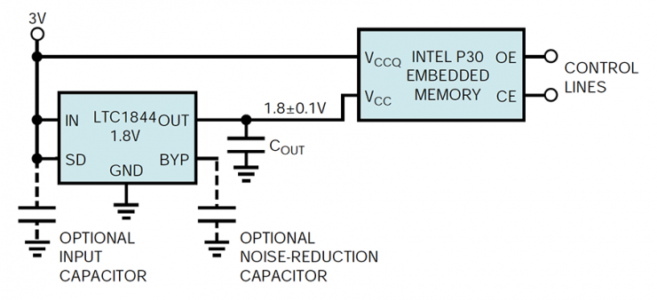
Figure 26. P30 Embedded memory regulators must maintain a 0.1V error band. The control line movement can result in a 50mA load step, so care must be taken in selecting COUT.
A load transient generator provides the output load test procedure (Trace A) of Figure 27. This test uses the circuit of Figure 8 and changes Q1's emitter current shunt to 1Ω. The regulator response, Trace B, shows only a 30mV peak error, more than twice as good as required. Increasing COUT to 10µF (Figure 28) reduces the peak output error to 12mV, almost six times the specification. However, a low-grade 10µF or 1µF, for that matter, capacitor produces the unwelcome surprise of Figure 29. Severe peak errors are observed on both edges, with 100mV observed on the falling edge. (The photo shows a sharpened version of the second half of Trace B to aid clarity.) This figure far exceeds the error budget and can lead to unreliable memory operation (References 4, 5, and 6).
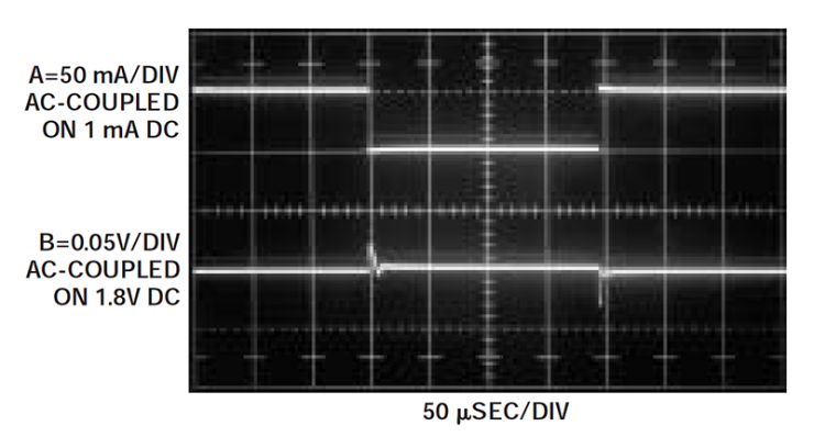
Figure 27. A 50mA load step (curve A) results in a 30mV regulator response peak, which is twice better than the error budget requirement. COUT is a low-loss 1µF capacitor.
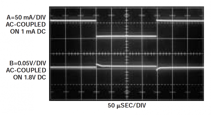
Figure 28 Increasing the value of C OUT to 10 µF reduces the regulator output peak to 12 mV, almost six times the required value.
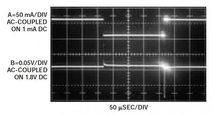
Figure 29. A low level of 10-µF FC OUT causes a 100-mV regulator output peak (curve B), violating the P30 regulator's memory limit. The oscilloscope photo enhances the second half of the trace for clarity.
- 12V to 28V DC-DC converter (based on LM2585)
- LM317 power supply circuit
- 30V/4A Adjustable Desktop Power Supply
- High-current LM317 regulated power supply
- Simple ±22V voltage regulator
- LM317 Adjustable Regulated Power Supply
- 1.5V to 5V converter
- Automatic battery charger
- Dual USB charger with switching regulator
- Gate drive transformers vs. high-side and low-side drivers: Where is power supply design headed?
- Importance of Voltage Supervisors and Output Topology Selection
- Design of adjustable DC stabilized power supply circuit module
- Power circuit of LBO-522 dual trace oscilloscope
- Power circuit with smoothing filter capacitor
- 500A-6V single-phase thyristor voltage regulating electroplating power supply circuit
- 300A-18V three-phase thyristor voltage regulating electrolytic power supply circuit
- Household emergency power circuit
- Inverter power circuit made with BJ50A
- Based on LM117 variable voltage regulator
- 5V voltage regulator circuit


 京公网安备 11010802033920号