MP5120, MP5220, MP5420
High Speed, +/-9V, Rail-to-Rail Input-Output
Op Amps
The Future of Analog IC Technology
DESCRIPTION
The MP5120 (single), MP5220 (dual), and
MP5420 (quad) are high-speed, high-voltage
rail-to-rail input-output amplifiers for use as
voltage reference buffers in Thin Film Transistor
Liquid Crystal Displays (TFT-LCDs). The
MP5120 family provides excellent overall
performance and versatility. The 20MHz –3dB
bandwidth and 45V/µs slew rate make these
amplifier
suitable
for
many
portable
applications.
The MP5120, MP5220, and MP5240 are
designed to operate at supply voltages as low
as 3.2V and up to 18V at 1.6mA of supply
current per amplifier. The input can swing 0.5V
below the negative rail and 0.5V above the
positive rail. The output can swing within
100mV of each rail.
The MP5420 quad channel is available in the
space-saving 14-pin TSSOP package. The
MP5220 dual channel is available in the 8-pin
MSOP package and the MP5120 single
channel is available in 5-pin TSOT package. All
feature a standard operational amplifier pin out.
FEATURES
•
•
•
•
•
•
•
•
•
•
•
•
•
•
•
•
•
•
•
•
•
•
•
Supply Operation: +/-9V
20MHz –3dB Bandwidth
45V/µs Slew Rate
Supply Current (per amplifier)1.6mA
Unity-Gain Stable
Output Swing within 100mV of Supply Rail
Rail-to-Rail Input Capability
High Output Drive Capability (50mA)
MP5120 Available in TSOT-5
MP5220 Available in MSOP-8
MP5420 Available in TSSOP14
TFT-LCD Drive Circuits
Electronic Notebooks
Electronic Games
Touch-Screen Displays
Personal Communication Devices
Personal Digital Assistants (PDA)
Portable Instrumentation
Sampling ADC Amplifiers
Wireless LAN
Office Automation
Active Filters
ADC/DAC Buffer
APPLICATIONS
“MPS” and “The Future of Analog IC Technology” are Registered Trademarks
of Monolithic Power Systems, Inc.
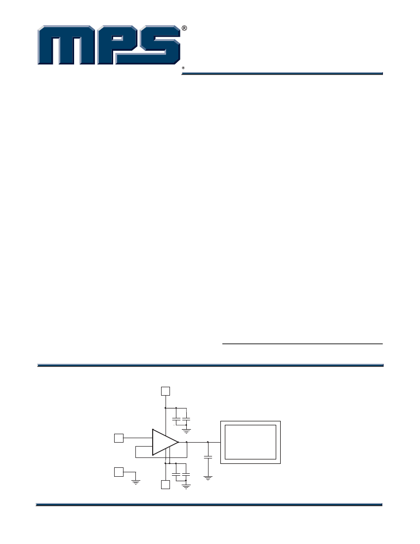
TYPICAL APPLICATION
Vs+
10uF
0.1nF
VIN+
U1
+
MP 5120
-
Co
GND
10uF
0.1nF
TFT LCD
Vs-
MP5120_MP5220_MP5420 Rev. 0.91
www.MonolithicPower.com
12/9/2009
MPS Proprietary Information. Unauthorized Photocopy and Duplication Prohibited.
© 2009 MPS. All Rights Reserved.
1
MP5120_MP5220_MP5420 –HIGH SPEED, +/-9V, RAIL-TO-RAIL INPUT-OUTPUT OP AMPS
ORDERING INFORMATION
Part Number*
MP5120DJ
MP5220DK
MP5420DM
Package
Top Marking
Free Air Temperature (T
A
)
TSOT
8F
–40°C to +85°C
MSOP
5220D
TSSOP
M5420DM
* For Tape & Reel, add suffix –Z (e.g. MP5120DJ–Z).
For RoHS Compliant packaging, add suffix –LF (e.g. MP5120DJ–LF–Z)
PACKAGE INFORMATION
MP5120
(5-PIN TSOT)
MP5220
(8-PIN MSOP)
TOP VIEW
VOUT 1
VS- 2
5 VS+
VOUTA
VINA-
4 VIN-
VINA+
VS-
MP5420
(14-PIN TSSOP)
1
2
3
TOP VIEW
8
7
6
VS+
VOUTB
VINB-
VINB+
--
--
+
+
VIN+ 3
TOP VIEW
VOUTA
VINA-
VINA+
VS+
VINB+
VINB-
VOUTB
1
2
3
4
5
6
7
--
--
--
--
14 VOUTD
13 VIND-
12 VIND+
11
VS-
+
+
10 VINC+
9 VINC-
8 VOUTC
MP5120_MP5220_MP5420 Rev. 0.91
www.MonolithicPower.com
12/9/2009
MPS Proprietary Information. Unauthorized Photocopy and Duplication Prohibited.
© 2009 MPS. All Rights Reserved.
+
4
--
5
+
+
2
MP5120_MP5220_MP5420 –HIGH SPEED, +/-9V, RAIL-TO-RAIL INPUT-OUTPUT OP AMPS
ABSOLUTE MAXIMUM RATINGS
(1)
(T
A
=25°C)
Supply Voltage between V
S+
and V
S-
.....................................................–0.3V to +22V
Input Voltage......................V
S-
- 0.5V, V
S+
+0.5V
Maximum Continuous Output Current
.................................................................. 50mA
Maximum Die Temperature ....................+125°C
Storage Temperature............... -60°C to +150°C
Ambient Operating Temp........... -40°C to +85°C
(2)
Power Dissipation. ...................... See Curves
Thermal Resistance
(4)
θ
JA
θ
JC
MSOP ....................................150 ...... 65.. °C/W
TSOT .....................................220 .... 110.. °C/W
TSSOT .....................................40 …… 6.. °C/W
Notes:
1) Exceeding these ratings may damage the device.
2) The maximum allowable power dissipation is a function of the
maximum junction temperature T
J
(MAX), the junction-to-
ambient thermal resistance
θ
JA
, and the ambient temperature
T
A
. The maximum allowable continuous power dissipation at
any ambient temperature is calculated by P
D
(MAX) = (T
J
(MAX)-T
A
)/θ
JA
. Exceeding the maximum allowable power
dissipation will cause excessive die temperature, and the
regulator will go into thermal shutdown. Internal thermal
shutdown circuitry protects the device from permanent
damage.
3) The device is not guaranteed to function outside of its
operating conditions.
4) Measured on JESD51-7, 4-layer PCB.
Recommended Operating Conditions
(3)
Power Supply Operation (V
S+
to V
S-
)
..........................................................3.2V to +18V
Operating Junct. Temp (T
J
) ....... -40°C to +125°C
MP5120_MP5220_MP5420 Rev. 0.91
www.MonolithicPower.com
12/9/2009
MPS Proprietary Information. Unauthorized Photocopy and Duplication Prohibited.
© 2009 MPS. All Rights Reserved.
3
MP5120_MP5220_MP5420 –HIGH SPEED, +/-9V, RAIL-TO-RAIL INPUT-OUTPUT OP AMPS
ELECTRICAL CHARACTERISTICS
V
S+
= +5V, V
S
- = -5V, R
L
= 10kΩ and C
L
= 10pF, T
A
=T
J
= 25°C, unless otherwise noted.
Parameter
INPUT CHARACTERISTICS
Input Offset Voltage
Average
Offset
Voltage
(3)
Drift
Input Bias Current
Input Impedance
Input Capacitance
Common-Mode Input Range
Common-Mode
Rejection
Ratio
Open Loop Gain
OUTPUT CHARACTERISTICS
Output Swing Low
Output Swing High
Short Circuit Current
Symbol
V
OS
TCV
OS
I
B
R
IN
C
IN
CMIR
CMRR
A
VOL
V
OL
V
OH
I
SC
for V
IN
from -5.5V to +5.5V
-4.5V
≤
V
OUT
≤
+4.5V
I
L
= -5mA
I
L
= -5mA
Sourcing
Sinking
V
S
is moved from ±2.25V to
±7.75V
No load
-4.0V
≤
V
OUT
≤
+4.0V, 20%
to 80%
(AV = +1), V
O
= 2V step
R
L
= 10kΩ, C
L
= 10pF
R
L
= 10kΩ, C
L
= 10pF
R
L
= 10kΩ, C
L
= 10pF
f = 5MHz (MP5220 &
MP5420 only)
70
-5.5
60
50
85
60
-4.95
4.82
70
130
95
1.6
≤
V
CM
=5V
Condition
V
CM
=5V
Min
Typ
2
5
0.5
1
1.35
+5.5
2
Max
20
Units
mV
µ/°C
µA
GΩ
pF
V
dB
dB
V
V
mA
POWER SUPPLY PERFORMANCE
Power
Supply
Rejection
PSRR
Ratio
Supply
Current
(Per
I
S
Amplifier)
DYNAMIC PERFORMANCE
Slew Rate (Rise/Fall)
Settling to +0.1% (A
V
= +1)
-3dB Bandwidth
Gain-Bandwidth Product
Phase Margin
Channel Separation
SR
t
S
BW
GBWP
PM
CS
dB
mA
45
500
20
14
50
70
V/µs
ns
MHz
MHz
dB
MP5120_MP5220_MP5420 Rev. 0.91
www.MonolithicPower.com
12/9/2009
MPS Proprietary Information. Unauthorized Photocopy and Duplication Prohibited.
© 2009 MPS. All Rights Reserved.
4
MP5120_MP5220_MP5420 –HIGH SPEED, +/-9V, RAIL-TO-RAIL INPUT-OUTPUT OP AMPS
TYPICAL PERFORMANCE CHARACTERISTICS
V
S+
=5V, V
S-
=-5V, R
L
=10KΩ, C
L
=12pF, T
A
=25ºC, unless otherwise noted.
Supply Current vs.
Supply Voltage
MP5120
1 .6
1 .4
20
15
10
V
OS
vs. V
IN
100
90
80
70
60
50
40
30
20
-3
-2
-1
0
1
2
3
4
PSRR vs. Frequency
Supply Current (mA)
1 .2
V
OS
(mV)
1
0 .8
0 .6
0 .4
0 .2
0
2
4
6
8
10 12 14 16 18
5
0
-5
-10
-15
-20
-4
PSRR ( dB )
10
0.1
10
1000
100000
Supply Voltage (V)
VIN ( V )
Fre que ncy (kHz )
Open Loop
80
60
200
180
160
140
50
40
30
Closed Loop Av=1
200
150
100
50
40
30
20
Closed Loop Av=2
200
150
Gain
100
50
0
Phase
-50
-100
-150
Gain (dB)
Gain (dB)
120
100
80
60
40
20
Gain (dB)
40
20
0
-20
-40
1
Phase
Gain
20
10
0
-1 0
-2 0
-3 0
-4 0
Gain
50
0
-50
10
0
-10
-20
-30
-40
Phase
-100
-150
10
100
0
1000 10000 100000
-5 0
-200
0.1 1 10 100 1000 10000 100000
Frequency (kHz)
-200
-50
0.1 1 10 100 1000 10000 100000
Frequency (kHz)
Frequency ( kHz )
Frequency Response vs. C
L
16
12
8
50pF
1000pF
100pF
Frequency Response vs. R
L
5
4
3
2
1
0
-1
-2
-3
-4
-5
Av=1
10
1000
100000
Output Noise vs. Frequency
MP5120
10000
Gain (dB)
4
0
-4
-8
-12
-16
1
10
Magnitude (dB)
10k
1k
560
560
150
1000
100
0pF
10
100
1000 10000 100000
0.1
1
0.1
10
1000
100000
Frequency (kHz)
Frequency (kHz)
Frequency (Hz)
MP5120_MP5220_MP5420 Rev. 0.91
www.MonolithicPower.com
12/9/2009
MPS Proprietary Information. Unauthorized Photocopy and Duplication Prohibited.
© 2009 MPS. All Rights Reserved.
5

 京公网安备 11010802033920号


