Datasheet
Operational Amplifiers
Low Noise Operational Amplifier
LM4559xxx
General Description
The LM4559xxx are low noise operational amplifiers
with high gain and wide bandwidth. They have good
performance of input referred noise voltage (5
nV/ Hz
)
and total harmonic distortion (0.0003%). These are
suitable for audio applications and active filter.
Features
High Voltage Gain
High Slew Rate
Low Noise Voltage
Low Total Harmonic Distortion
Low Power Consumption
Application
Audio Application
Consumer Equipment
Active Filter
Key Specifications
Operating Supply Voltage:
Temperature Range:
Voltage Gain:
Unity Gain Bandwidth:
Slew Rate:
Input Referred Noise Voltage:
Package
SOP-8
SOP-J8
SSOP-B8
TSSOP-B8
MSOP8
TSSOP-B8J
±4V to ±18V
-40°C to +85°C
110dB (Typ)
3.3MHz (Typ)
3.5V/µs (Typ)
5
nV/ Hz
(Typ)
W(Typ) xD(Typ) xH(Max)
5.00mm x 6.20mm x 1.71mm
4.90mm x 6.00mm x 1.65mm
3.00mm x 6.40mm x 1.35mm
3.00mm x 6.40mm x 1.20mm
2.90mm x 4.00mm x 0.90mm
3.00mm x 4.90mm x 1.10mm
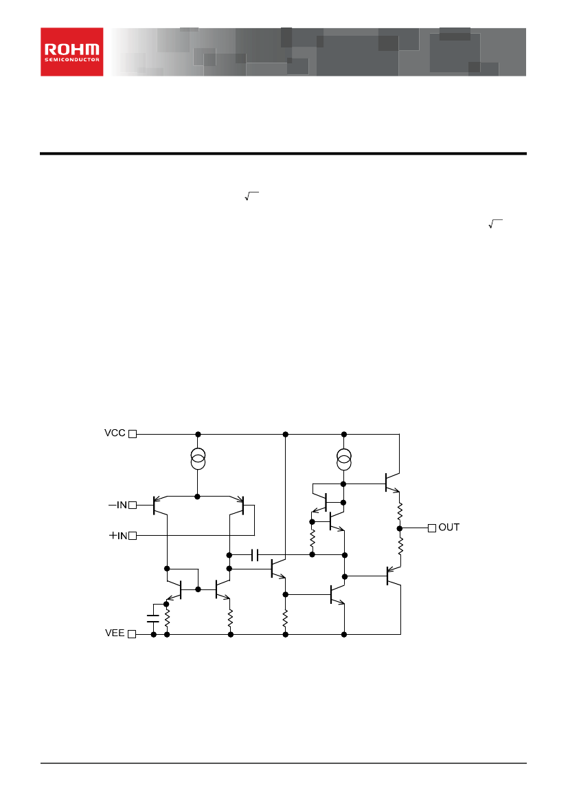
Simplified Schematic
Figure 1. Simplified Schematic (1 channel only)
○Product
structure:Silicon monolithic integrated circuit
www.rohm.com
©2012 ROHM Co., Ltd. All rights reserved.
TSZ22111½14½001
○This
product has no designed protection against radioactive rays.
1/25
TSZ02201-0RAR1G200580-1-2
04.Dec.2013 Rev.003
LM4559xxx
Absolute Maximum Ratings
(T
A
=25°C)
Parameter
Supply Voltage
Symbol
VCC – VEE
SOP8
SOP-J8
Power Dissipation
P
D
SSOP-B8
TSSOP-B8
MSOP8
TSSOP-B8J
Differential Input Voltage
(Note 6)
Input Common-mode
Voltage Range
Operating Supply Voltage
Operating Temperature
Storage Temperature
Maximum
Junction Temperature
V
ID
V
ICM
V
opr
T
opr
T
stg
T
Jmax
Rating
+36
0.68
(Note 1,5)
Datasheet
Unit
V
0.67
(Note 2,5)
0.62
(Note 3,5)
0.62
(Note 3,5)
0.58
(Note 4,5)
0.58
(Note 4,5)
+36
(VEE - 0.3) to (VEE + 36)
±4 to ±18
-40 to +85
-55 to +150
+150
V
V
V
°C
°C
°C
W
(Note 1) When used at temperature above T
A
=25°C, reduce by 5.5mW/°C.
(Note 2) When used at temperature above T
A
=25°C, reduce by 5.4mW/°C.
(Note 3) When used at temperature above T
A
=25°C, reduce by 5.0mW/°C.
(Note 4) When used at temperature above T
A
=25°C, reduce by 4.7mW/°C.
(Note 5) Mounted on a FR4 glass epoxy PCB(70mm×70mm×1.6mm).
(Note 6) The differential input voltage is the voltage difference between inverting input and non-inverting input.
Input terminal voltage is set to more than VEE.
Caution: Absolute maximum rating of each item indicates the condition which must not be exceeded.
Application of voltage in excess of absolute maximum rating or usage out of absolute maximum rated
temperature environment may cause deterioration of characteristics.
www.rohm.com
©2012 ROHM Co., Ltd. All rights reserved.
TSZ22111½15½001
3/25
TSZ02201-0RAR1G200580-1-2
04.Dec.2013 Rev.003
LM4559xxx
Datasheet
Description of Electrical Characteristics
Described here are the terms of electric characteristics used in this datasheet. Items and symbols used are also shown.
Note that item name, symbol and their meaning may differ from those on other manufacturer’s document or general
documents.
1. Absolute maximum ratings
Absolute maximum rating items indicate the condition which must not be exceeded. Application of voltage in excess of absolute
maximum rating or use out of absolute maximum rated temperature environment may cause deterioration of characteristics.
(1) Supply Voltage (VCC/VEE)
Indicates the maximum voltage that can be applied between the positive power supply terminal and negative power
supply terminal without deterioration or destruction of characteristics of internal circuit.
(2) Differential Input Voltage (V
ID
)
Indicates the maximum voltage that can be applied between non-inverting and inverting terminals without damaging
the IC.
(3) Input Common-mode Voltage Range (V
ICM
)
Indicates the maximum voltage that can be applied to the non-inverting and inverting terminals without deterioration
or destruction of electrical characteristics. Input common-mode voltage range of the maximum ratings does not assure
normal operation of IC. For normal operation, use the IC within the input common-mode voltage range characteristics.
(4) Power dissipation (P
D
)
Indicates the power that can be consumed by the IC when mounted on a specific board at the ambient temperature 25℃
(normal temperature). As for package product, Pd is determined by the temperature that can be permitted by the IC in
the package (maximum junction temperature) and the thermal resistance of the package.
2. Electrical characteristics item
(1) Input Offset Voltage (V
IO
)
Indicates the voltage difference between non-inverting terminal and inverting terminals. It can be translated into the
input voltage difference required for setting the output voltage at 0 V.
(2) Input Offset Current (I
IO
)
Indicates the difference of input bias current between the non-inverting and inverting terminals.
(3) Input Bias Current (I
B
)
Indicates the current that flows into or out of the input terminal. It is defined by the average of input bias currents at
the non-inverting and inverting terminals.
(4) Input Common-mode Voltage Range (V
ICM
)
Indicates the input voltage range where IC operates normally.
(5) Maximum Output Voltage (V
OM
)
Indicates the voltage range that the IC can output under specified load condition. It is typically divided into high-level
output voltage and low-level output voltage. High-level output voltage indicates the upper limit of output voltage.
Low-level output voltage indicates the lower limit.
(6) Large Signal Voltage Gain (A
V
)
Indicates the amplifying rate (gain) of output voltage against the voltage difference between non-inverting terminal
and inverting terminal. It is normally the amplifying rate (gain) with reference to DC voltage.
Av = (Output voltage) / (Differential Input voltage)
(7) Supply Current (I
CC
)
Indicates the current that flows within the IC under specified no-load conditions.
(8) Output Source Current/ Output Sink Current (I
source
/ I
sink
)
The maximum current that can be output from the IC under specific output conditions. The output source current
indicates the current flowing out from the IC, and the output sink current indicates the current flowing into the IC.
(9) Unity Gain Frequency (f
T
)
Indicates a frequency where the voltage gain of operational amplifier is 1.
(10) Gain Bandwidth (GBW)
Indicates to multiply by the frequency and the gain where the voltage gain decreases 6dB/octave.
(11) Phase Margin (θ)
Indicates the margin of phase from 180 degree phase lag at unity gain frequency.
(12) Common-mode Rejection Ratio (CMRR)
Indicates the ratio of fluctuation of input offset voltage when the input common-mode voltage is changed. It is
normally the fluctuation of DC.
CMRR = (Change of Input common-mode voltage)/(Input offset fluctuation)
(13) Power Supply Rejection Ratio (PSRR)
Indicates the ratio of fluctuation of input offset voltage when supply voltage is changed.
It is normally the fluctuation of DC.
PSRR= (Change of power supply voltage)/(Input offset fluctuation)
(14) Input Referred Noise Voltage (V
N
)
Indicates a noise voltage generated inside the operational amplifier reflected back to an ideal voltage source
connected in series with the input terminal.
(15) Total Harmonic Distortion + Noise (THD+N)
Indicates the fluctuation of input offset voltage or that of output voltage with reference to the change of output voltage
of driven channel.
www.rohm.com
©2012 ROHM Co., Ltd. All rights reserved.
TSZ22111½15½001
5/25
TSZ02201-0RAR1G200580-1-2
04.Dec.2013 Rev.003
 京公网安备 11010802033920号


