M54HCT08
M74HCT08
QUAD 2-INPUT AND GATE
.
.
.
.
.
.
.
HIGH SPEED
t
PD
= 12 ns (TYP.) AT V
CC
= 5 V
LOW POWER DISSIPATION
I
CC
= 1
µA
(MAX.) AT T
A
= 25
°C
COMPATIBLE WITH TTL OUTPUTS
V
IH
= 2V (MIN.) V
IL
= 0.8V (MAX)
OUTPUT DRIVE CAPABILITY
10 LSTTL LOADS
SYMMETRICAL OUTPUT IMPEDANCE
I
OH
= I
OL
= 4 mA (MIN.)
BALANCED PROPAGATION DELAYS
t
PLH
= t
PHL
PIN AND FUNCTION COMPATIBLE
WITH 54/74LS08
B1R
(Plastic Package)
F1R
(Ceramic Package)
M1R
(Micro Package)
C1R
(Chip Carrier)
DESCRIPTION
The M54/74HCT08 is a high speed CMOS QUAD
2-INPUT AND GATE fabricated in silicon gate
C
2
MOS technology. It has the same high speed per-
formance of LSTTL combined with true CMOS low
power consumption. The internal circuit is com-
posed of 2 stages including buffer output, which
gives high noise immunity and stable output. All in-
puts are equipped with protection circuits against
static discharge and transient excess voltage.
This integrated circuit has input and output charac-
teristics that are fully compatible with 54/74 LSTTL
logic families. M54/74HC devices are designed to
directly interface HSC
2
MOS systems with TTL and
NMOS components. They are also plug in replace-
ments for LSTTL devices giving a reduction of
power consumption.
INPUT AND OUTPUT EQUIVALENT CIRCUIT
ORDER CODES :
M54HCT08F1R
M74HCT08M1R
M74HCT08B1R
M74HCT08C1R
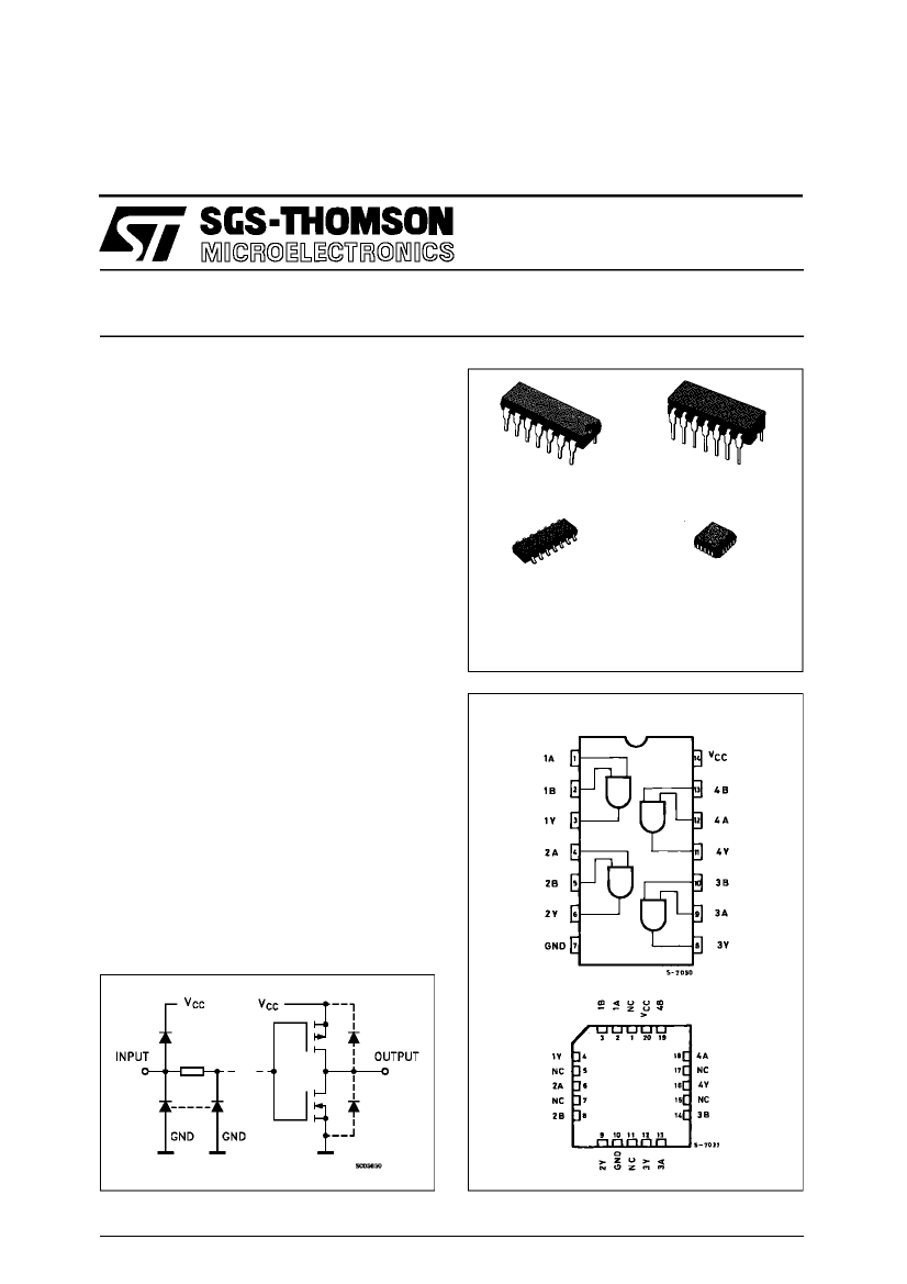
PIN CONNECTIONS
(top view)
NC =
No Internal
Connection
February 1993
1/9
M54/M74HCT08
TRUTH TABLE
A
L
L
H
H
B
L
H
L
H
Y
L
L
L
H
IEC LOGIC SYMBOL
PIN DESCRIPTION
PIN No
1, 4, 9, 12
2, 5, 10, 13
3, 6, 8, 11
7
14
SYMBOL
1A to 4A
1B to 4B
1Y to 4Y
GND
V
CC
NAME AND FUNCTION
Data Inputs
Data Inputs
Data Outputs
Ground (0V)
Positive Supply Voltage
SCHEMATIC CIRCUIT
(Per Gate)
ABSOLUTE MAXIMUM RATING
Symbol
V
CC
V
I
V
O
I
IK
I
OK
I
CC
I
O
or I
GND
P
D
T
stg
T
L
Supply Voltage
DC Input Voltage
DC Output Voltage
DC Input Diode Current
DC Output Diode Current
DC Output Source Sink Current Per Output Pin
DC V
CC
or Ground Current
Power Dissipation
Storage Temperature
Lead Temperature (10 sec)
Parameter
Value
-0.5 to +7
-0.5 to V
CC
+ 0.5
-0.5 to V
CC
+ 0.5
±
20
±
20
±
25
±
50
500 (*)
-65 to +150
300
Unit
V
V
V
mA
mA
mA
mA
mW
o
o
C
C
Absolute Maximum Ratings are those values beyond which damage to the device may occur. Functional operation under these condition isnotimplied.
(*) 500 mW:
≅
65
o
C derate to 300 mW by 10mW/
o
C: 65
o
C to 85
o
C
2/9
M54/M74HCT08
AC ELECTRICAL CHARACTERISTICS
(C
L
= 50 pF, Input t
r
= t
f
= 6 ns)
Test Conditions
Symbol
Parameter
V
CC
(V)
4.5
4.5
T
A
= 25 C
54HC and 74HC
Min. Typ. Max.
8
13
5
38
15
21
10
o
Value
-40 to 85
o
C -55 to 125
o
C
74HC
54HC
Min. Max. Min. Max.
19
26
10
22
32
10
Unit
t
TLH
t
THL
t
PLH
t
PHL
C
IN
C
PD
(*)
Output Transition
Time
Propagation
Delay Time
Input Capacitance
Power Dissipation
Capacitance
ns
ns
pF
pF
(*) C
PD
is defined as the value of the IC’s internal equivalent capacitance which is calculated from the operating current consumption without load.
(Refer to Test Circuit). Average operting current can be obtained by the following equation. I
CC
(opr) = C
PD
•V
CC
•f
IN
+ I
CC
/4 (per Gate)
SWITCHING CHARACTERISTICS TEST CIRCUIT
TEST CIRCUIT I
CC
(Opr.)
INPUT WAVEFORM IS THE SAME AS THAT IN CASE OF SWITCHING CHARACTERISTICS TEST.
4/9
 京公网安备 11010802033920号


