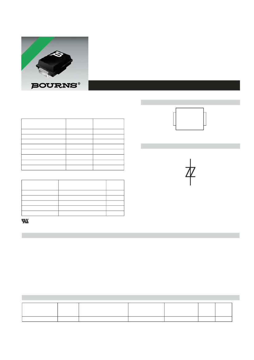
LOW CAPACITANCE BIDIRECTIONAL THYRISTOR OVERVOLTAGE PROTECTORS
| TISP4CXXXH3BJ | TISP4C145H3BJ | TISP4C350H3BJ | TISP4C290H3BJ | TISP4C395H3BJ | TISP4C250H3BJ | TISP4C220H3BJ | TISP4C180H3BJ | TISP4C125H3BJ | |
|---|---|---|---|---|---|---|---|---|---|
| Description | LOW CAPACITANCE BIDIRECTIONAL THYRISTOR OVERVOLTAGE PROTECTORS | LOW CAPACITANCE BIDIRECTIONAL THYRISTOR OVERVOLTAGE PROTECTORS | LOW CAPACITANCE BIDIRECTIONAL THYRISTOR OVERVOLTAGE PROTECTORS | LOW CAPACITANCE BIDIRECTIONAL THYRISTOR OVERVOLTAGE PROTECTORS | LOW CAPACITANCE BIDIRECTIONAL THYRISTOR OVERVOLTAGE PROTECTORS | LOW CAPACITANCE BIDIRECTIONAL THYRISTOR OVERVOLTAGE PROTECTORS | LOW CAPACITANCE BIDIRECTIONAL THYRISTOR OVERVOLTAGE PROTECTORS | LOW CAPACITANCE BIDIRECTIONAL THYRISTOR OVERVOLTAGE PROTECTORS | LOW CAPACITANCE BIDIRECTIONAL THYRISTOR OVERVOLTAGE PROTECTORS |
| Is it lead-free? | - | Contains lead | Contains lead | Contains lead | Contains lead | Contains lead | Contains lead | Contains lead | Contains lead |
| Is it Rohs certified? | - | incompatible | incompatible | incompatible | incompatible | incompatible | incompatible | incompatible | incompatible |
| package instruction | - | SMALL OUTLINE, R-PDSO-G2 | SMALL OUTLINE, R-PDSO-G2 | SMALL OUTLINE, R-PDSO-G2 | SMALL OUTLINE, R-PDSO-C2 | SMALL OUTLINE, R-PDSO-G2 | SMALL OUTLINE, R-PDSO-G2 | SMALL OUTLINE, R-PDSO-G2 | SMALL OUTLINE, R-PDSO-G2 |
| Contacts | - | 2 | 2 | 2 | 2 | 2 | 2 | 2 | 2 |
| Reach Compliance Code | - | _compli | _compli | _compli | _compli | _compli | _compli | _compli | _compli |
| ECCN code | - | EAR99 | - | EAR99 | - | EAR99 | EAR99 | EAR99 | EAR99 |
| Other features | - | UL RECOGNIZED | UL RECOGNIZED | UL RECOGNIZED | UL RECOGNIZED | UL RECOGNIZED | UL RECOGNIZED | UL RECOGNIZED | UL RECOGNIZED |
| Maximum breakover voltage | - | 145 V | 350 V | 290 V | 395 V | 250 V | 220 V | 180 V | 125 V |
| Configuration | - | SINGLE | SINGLE | SINGLE | SINGLE | SINGLE | SINGLE | SINGLE | SINGLE |
| Maximum off-state DC voltage | - | 120 V | 275 V | 220 V | 320 V | 190 V | 180 V | 145 V | 100 V |
| JESD-30 code | - | R-PDSO-G2 | R-PDSO-G2 | R-PDSO-G2 | R-PDSO-C2 | R-PDSO-G2 | R-PDSO-G2 | R-PDSO-G2 | R-PDSO-G2 |
| On-state non-repetitive peak current | - | 30 A | 30 A | 30 A | 30 A | 30 A | 30 A | 30 A | 30 A |
| Number of components | - | 1 | 1 | 1 | 1 | 1 | 1 | 1 | 1 |
| Number of terminals | - | 2 | 2 | 2 | 2 | 2 | 2 | 2 | 2 |
| Maximum operating temperature | - | 150 °C | 150 °C | 150 °C | 150 °C | 150 °C | 150 °C | 150 °C | 150 °C |
| Minimum operating temperature | - | -40 °C | -40 °C | -40 °C | -40 °C | -40 °C | -40 °C | -40 °C | -40 °C |
| Package body material | - | PLASTIC/EPOXY | PLASTIC/EPOXY | PLASTIC/EPOXY | PLASTIC/EPOXY | PLASTIC/EPOXY | PLASTIC/EPOXY | PLASTIC/EPOXY | PLASTIC/EPOXY |
| Package shape | - | RECTANGULAR | RECTANGULAR | RECTANGULAR | RECTANGULAR | RECTANGULAR | RECTANGULAR | RECTANGULAR | RECTANGULAR |
| Package form | - | SMALL OUTLINE | SMALL OUTLINE | SMALL OUTLINE | SMALL OUTLINE | SMALL OUTLINE | SMALL OUTLINE | SMALL OUTLINE | SMALL OUTLINE |
| Peak Reflow Temperature (Celsius) | - | NOT SPECIFIED | NOT SPECIFIED | NOT SPECIFIED | NOT SPECIFIED | NOT SPECIFIED | NOT SPECIFIED | NOT SPECIFIED | NOT SPECIFIED |
| Certification status | - | Not Qualified | Not Qualified | Not Qualified | Not Qualified | Not Qualified | Not Qualified | Not Qualified | Not Qualified |
| surface mount | - | YES | YES | YES | YES | YES | YES | YES | YES |
| Terminal form | - | GULL WING | GULL WING | GULL WING | C BEND | GULL WING | GULL WING | GULL WING | GULL WING |
| Terminal location | - | DUAL | DUAL | DUAL | DUAL | DUAL | DUAL | DUAL | DUAL |
| Maximum time at peak reflow temperature | - | NOT SPECIFIED | NOT SPECIFIED | NOT SPECIFIED | NOT SPECIFIED | NOT SPECIFIED | NOT SPECIFIED | NOT SPECIFIED | NOT SPECIFIED |
| Trigger device type | - | SILICON SURGE PROTECTOR | SILICON SURGE PROTECTOR | SILICON SURGE PROTECTOR | SILICON SURGE PROTECTOR | SILICON SURGE PROTECTOR | SILICON SURGE PROTECTOR | SILICON SURGE PROTECTOR | SILICON SURGE PROTECTOR |
| Base Number Matches | - | 1 | 1 | 1 | 1 | 1 | 1 | 1 | 1 |
 京公网安备 11010802033920号


