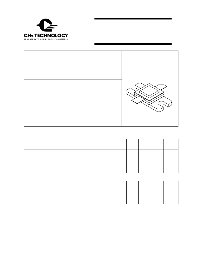
RF Power Bipolar Transistor, 1-Element, S Band, Silicon, NPN, HERMETIC SEALED, 55AW, 2 PIN
| Parameter Name | Attribute value |
| Is it lead-free? | Contains lead |
| Is it Rohs certified? | incompatible |
| Objectid | 2121115649 |
| package instruction | HERMETIC SEALED, 55AW, 2 PIN |
| Contacts | 2 |
| Reach Compliance Code | unknown |
| ECCN code | EAR99 |
| Other features | HIGH RELIABILITY |
| Maximum collector current (IC) | 3 A |
| Configuration | SINGLE |
| highest frequency band | S BAND |
| JESD-30 code | R-CDFM-F2 |
| JESD-609 code | e0 |
| Number of components | 1 |
| Number of terminals | 2 |
| Maximum operating temperature | 200 °C |
| Package body material | CERAMIC, METAL-SEALED COFIRED |
| Package shape | RECTANGULAR |
| Package form | FLANGE MOUNT |
| Polarity/channel type | NPN |
| Certification status | Not Qualified |
| surface mount | YES |
| Terminal surface | TIN LEAD |
| Terminal form | FLAT |
| Terminal location | DUAL |
| transistor applications | AMPLIFIER |
| Transistor component materials | SILICON |
 京公网安备 11010802033920号


