FUJITSU SEMICONDUCTOR
DATA SHEET
DS04-13501-3E
Linear IC General purpose Converter
CMOS
D/A Converter for Digital Tuning
(12 channels. 8-bit, with OP amplifier)
MB88346B
■
DESCRIPTION
The MB88346B features 12 channels of 8-bit D/A converters with output amplifier for digital tuning. The output
amplifier provides high current drive capability.
As the MB88346B inputs data in serial, it requires only three control lines and can also be cascade-connected
with the MB88340 series.
The MB88346B is suitable for electronic volumes and replacement for potentiometers for adjustment, in addition
to normal D/A converter applications.
■
FEATURES
• Low power consumption
• Small package
• Integrating 12 channels of R-2R type 8-bit D/A converter
(Continued)
■
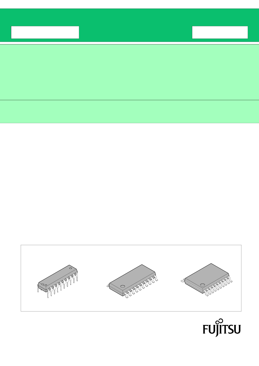
PACKAGES
20-pin plastic DIP
20-pin plastic SOP
20-pin plastic SSOP
(DIP-20P-M02)
(FPT-20P-M01)
(FPT-20P-M03)
MB88346B
(Continued)
• Built-in analog output amplifier (Max
+1.0
mA sink/source current)
• Analog output range : 0 to V
CC
• The range of D/A conversion can be independently set by separated the power supply for MCU interface and
OP amplifier and the power supply for D/A converter.
• Capable of being controlled directly by a 3-V MCU (input voltage : “H”
=
0.5 V
CC
, “L”
=
0.2 V
CC
)
• Serial data input, 2.5 MHz operation
• CMOS process
• Package lineup : DIP 20-pin, SOP 20-pin, SSOP 20-pin
2
MB88346B
■
PIN ASSIGNMENTS
(TOP VIEW)
V
SS
AO
3
AO
4
AO
5
AO
6
AO
7
AO
8
AO
9
AO
10
V
DD
1
2
3
4
5
6
7
8
9
10
20
19
18
17
16
15
14
13
12
11
GND
AO
2
AO
1
DI
CLK
LD
DO
AO
12
AO
11
V
CC
V
SS
AO
3
AO
4
AO
5
AO
6
AO
7
AO
8
AO
9
AO
10
V
DD
1
2
3
4
5
6
7
8
9
10
(TOP VIEW)
20
19
18
17
16
15
14
13
12
11
GND
AO
2
AO
1
DI
CLK
LD
DO
AO
12
AO
11
V
CC
(DIP-20P-M02)
(FPT-20P-M01)
(FPT-20P-M03)
■
PIN DESCRIPTION
Pin No.
17
14
16
15
18,
19,
2,
3,
4,
5,
6,
7,
8,
9,
12,
13
11
20
10
1
Symbol
DI*
DO
CLK*
LD*
AO
1
,
AO
2
,
AO
3
,
AO
4
,
AO
5
,
AO
6
,
AO
7
,
AO
8
,
AO
9
,
AO
10
,
AO
11
,
AO
12
V
CC
GND
V
DD
V
SS
I/O
I
O
I
I
Pin name
Data input pin
Data output pin
Shift clock input pin
Load signal input pin
Function
This pin inputs 12-bit serial data.
This pin outputs MSB bit data of 12-bit shift register.
Input signal from DI pin is inputted to 12-bit shift register
at rising of shift clock.
If input “H” level to LD pin, the data of 12-bit shift register
is loaded to the decoder and the register for D/A output.
O
D/A output pin
These pins output analog data of 8-bit D/A converter with
OP amplifier.
⎯
⎯
⎯
⎯
Power supply pin
Ground pin
Power supply pin
Ground pin
Power supply pin of MCU interface and OP amplifier
Ground pin of MCU interface and OP amplifier
Power supply pin of D/A converter
Ground pin of D/A converter
* : When three pins, DI, CLK, and LD pins are connected to 3-V MCU, they are fixed to “L” level at non transfer.
3
MB88346B
■
BLOCK DIAGRAM
V
CC
GND
DI
CLK
D0
D1
D2
D3
12-bit shift register
D4
D5
D6
D7
D8
D9
D10 D11
DO
8
12
Address decoder
1 2 3 4
D0
12
12
D7
LD
D0
1
D7
8-bit latch
8-bit
R-2R
D/A converter
8-bit latch
8-bit
R-2R
D/A converter
+
_
+
−
V
CC
GND
AO
1
AO
12
V
DD
V
SS
4
MB88346B
■
DATA FOR CHIP CONTROL
1. Data for Shift Register
• The chip is controlled by 12 bits of data input to the shift register.
• The shift register inputs a total of 12 bits of data consisting of a four-bit address selection signal and an eight-
bit D/A converter control signal.
• A data to the shift register is inputted to the DI pin in the order of D11 (MSB) to D0 (LSB) .
Last (LSB)
D0
D1
D2
D3
D4
D5
D6
D7
D8
D9
First (MSB)
D10
D11
D/A converter control signal
Address selected signal
2. D/A Converter Control Signal
Input data signal
D0
0
1
0
1
0
1
D1
0
0
1
1
1
1
D2
0
0
0
0
1
1
D3
0
0
0
0
1
1
D4
0
0
0
0
1
1
D5
0
0
0
0
1
1
D6
0
0
0
0
1
1
D7
0
0
0
0
1
1
D/A converter output voltage
≅
V
SS
≅
V
REF
/
255
×
1
+
V
SS
≅
V
REF
/
255
×
2
+
V
SS
≅
V
REF
/
255
×
3
+
V
SS
≅
V
REF
/
255
×
254
+
V
SS
≅
V
DD
V
REF
= V
DD
- V
SS
5
 京公网安备 11010802033920号


