RN73
ultra precision 0.05%, 0.1%, 1% tolerance
thin film chip resistor
EU
features
•
Nickel chromium thin film resistor element
•
Products with lead-free terminations meet
EU RoHS requirements
% Rated Power
60
40
20
0
-60 -40
-55
% Rated Power
resistors
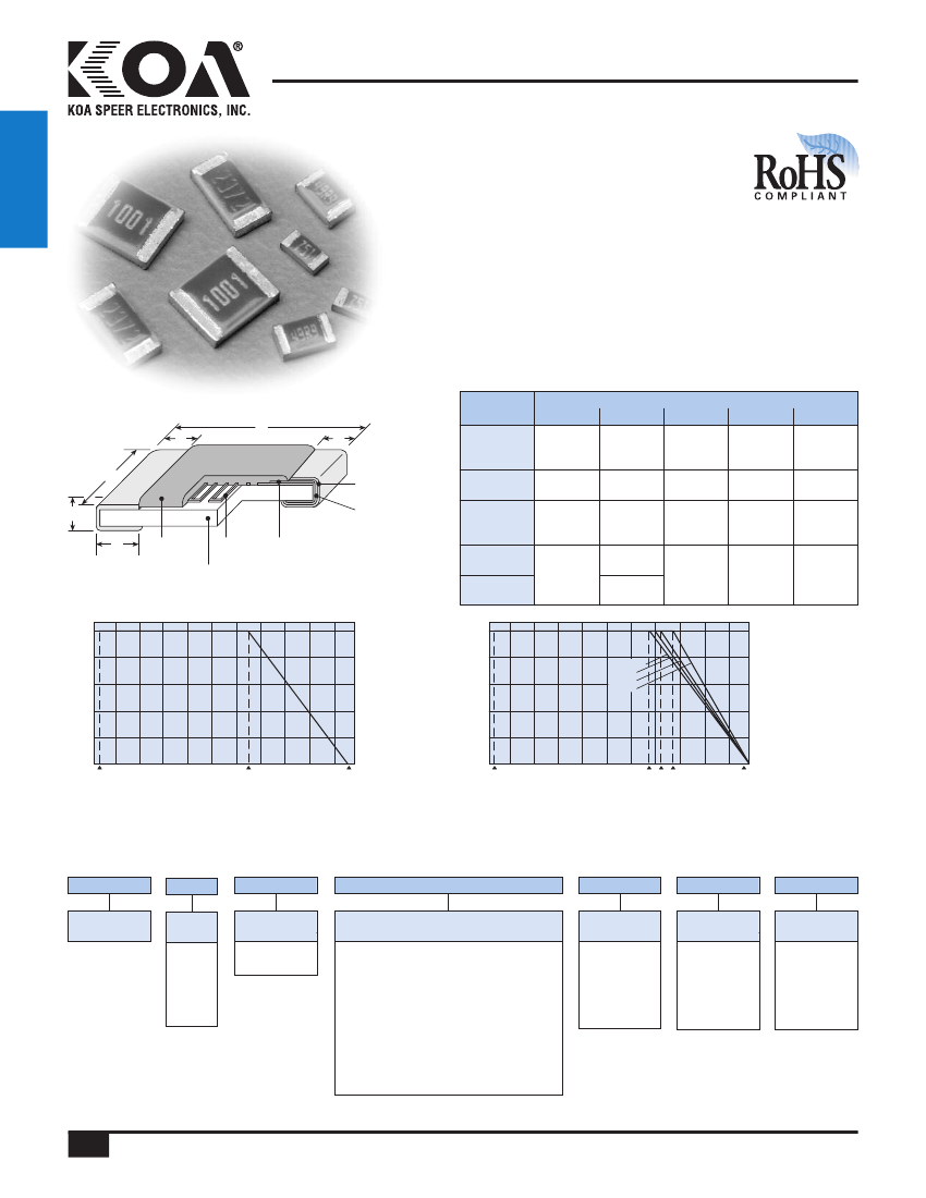
dimensions and construction
c
L
c
Type
(Inch Size Code)
L
.039
+.004
-.002
(1.0
+0.1
)
-0.05
Dimensions
inches
(mm)
W
c
d
.02±.002 .008±.004
(0.5±0.05) (0.2±0.1)
.01
+.002
-.004
(0.25
+0.05
)
-0.1
t
.014±.002
(0.35±0.05)
RN73 1E
(0402)
Solder
Plating
Ni
Plating
W
RN73 1J
(0603)
RN73 2A
(0805)
RN73 2B
(1206)
RN73 2E
(1210)
100
80
60
40
20
0
-60 -40
-55
.063±.008 .031±.004 .012±.004 .012±.004 .018±.004
(1.6±0.2)
(0.8±0.1)
(0.3±0.1) (0.45±0.1)
(0.3±0.1)
.079±.008 .049±.008 .016±.008
(2.0±0.2) (1.25±0.2) (0.4±0.2)
.063±.008
.126±.008
(1.6±0.2)
(3.2±0.2)
.098±.008
(2.5±0.2)
.02±.012
(0.5±0.3)
.012
(0.3
.016
(0.4
+.008
-.004
+0.2
)
-0.1
+.008
-.004
+0.2
-0.1
)
t
d
Protective
Coating
Resistive Inner
Film
Electrode
.02±.004
(0.5±0.1)
.024±.004
(0.6±0.1)
Ceramic
Substrate
Derating Curve
100
80
1E, 1J (75°C)
2A (80°C)
2B (85°C)
2E (95°C)
-20
0
20
40
60
80
100
70
Ambient Temperature
(°C)
120 140
155
-20
0
80
100 120 140
75 85 95
155
Terminal Part Temperature
(°C)
40
60
20
For resistors operated at an ambient temperature of 70°C or above, a
power rating shall be derated in accordance with the above derating curve.
ordering information
RN73
Type
2B
Size
1E
1J
2A
2B
2E
T
Termination
Material
T: Sn
L: SnPb
TE
For resistors operated terminal part temperature of described for each size
or above, a power rating shall be derated in accordance with derating curve.
Please refer to “Introduction of the derating curves based on the terminal
part temperature” in the beginning of our catalog before use.
1002
Nominal
Resistance
3 significant
figures + 1
multiplier
“R” indicates
decimal on
value <100Ω
B
Tolerance
A: ±0.05%
B: ±0.1%
C: ±0.25%
D: ±0.5%
F: ±1.0%
25
T.C.R.
(ppm/°C)
05
10
25
50
100
Packaging
TP: 0402: 7" 2mm pitch punch paper
TD: 0603, 0805, 1206, 1210:
7" 4mm pitch punched paper
TDD: 0603, 0805, 1206, 1210:
10" paper tape
TE: 0805, 1206, 1210:
7" embossed plastic
TED: 0805, 1206, 1210:
10" embossed plastic
For further information on packaging,
please refer to Appendix A
Specifications given herein may be changed at any time without prior notice. Please confirm technical specifications before you order and/or use.
11/06/17
38
KOA Speer Electronics, Inc.
• 199 Bolivar Drive • Bradford, PA 16701 • USA • 814-362-5536 • Fax: 814-362-8883 • www.koaspeer.com
RN73
ultra precision 0.05%, 0.1%, 1% tolerance
thin film chip resistor
resistors
applications and ratings
Power Rating
1
Rated
Resistance Range (Ω)
Rated
T.C.R.
@ 70°C
Terminal
Part
E-24, E-96, E-192*
Ambient
(ppm/°C)
High
Part
Designation
Max.
General Power Temp.
(A±0.05%) (B±0.1%) (C±0.25%) (D±0.5%)
Temp.
—
±25
100 - 100k 100 - 100k 10 - 120k
RN731E
70°C
75°C
.063W
—
±50
100 - 100k 100 - 100k 10 - 120k
—
±5
100 - 47k
—
—
1K - 47k
1K - 47k
±10
100 - 47k 100 - 47k 100 - 47k
RN731J
15 - 360k
15 - 360k 10 - 360k
70°C
75°C
.063W
.1W
±25
1K - 47k
±50
—
15 - 360k 15 - 360k 10 - 360k
±100
±5
±10
±25
±50
±100
±5
±10
±25
±50
±100
±10
±25
±50
±100
—
100 - 100k
100 - 100k
51 - 100k
—
—
100 - 300k
100 - 300k
51 - 300k
—
—
100 - 510k
51 - 510k
—
—
—
100 - 100k
100 - 100k
15 - 1M
15 - 1M
—
100 - 300k
100 - 300k
15 - 1M
15 - 1M
—
100 - 510k
15 - 1M
15 - 1M
—
—
—
100 - 100k
15 - 1M
15 - 1M
—
—
100 - 300k
15 - 1M
15 - 1M
—
100 - 510k
15 - 1M
15 - 1M
—
10 - 360k
—
100 - 100k
10 - 1M
10 - 1M
10 - 1M
—
100 - 300k
10 - 1M
10 - 1M
10 - 1M
100 - 510k
10 - 1M
10 - 1M
10 - 1M
Absolute Absolute
Max.
Max.
Working Overload
(F±1.0%) Voltage Voltage
10 - 120k
50V
100V
10 - 120k
—
100 - 47k
75V
150V
10 - 360k
10Ω - 360k
10 - 360k
—
100 - 100k
10 - 1M
10 - 1M
10 - 1M
—
100 - 300k
10 - 1M
10 - 1M
10 - 1M
100 - 510k
10 - 1M
10 - 1M
10 - 1M
RN732A
.1W
.125W
70°C
80°C
150V
300V
RN732B
.125W
.25W
70°C
85°C
200V
400V
RN732E
.25W
—
70°C
95°C
200V
400V
1
* No marking on E-192 values
Operating Temperature Range: -55°C to +155°C
Reliability performance is different. Please confirm the performance table.
If any questions should arise whether to use the “Rated Ambient Temperature” or the “Rated Terminal Part Temperature”, please give priority to the “Rated Terminal
Part Temperature.” Prior to use and for more details refer to “Introduction of the derating curves on the terminal part temperature” in the beginning of the catalog.
environmental applications
Performance Characteristics
Parameter
Resistance
T.C.R.
Overload (Short time)
Resistance to Solder Heat
Rapid Change of Temperature
Moisture Resistance
Endurance at 70°C
High Temperature Exposure
Requirement
∆
R ±(%+0.05Ω)
Limit
Typical
Within specified
—
tolerance
Within specified
—
T.C.R.
General: ±0.1%
High Power: ±0.5%
±0.01%
±0.03%
Test Method
25°C
+25°C/+125°C: T.C.R. = ±5 (X10
-6
/K)
+25°C/-55°C and +25°C/+125°C: all others
Rated Voltage x 2.5 or Max. overload voltage, whichever is less for 5 seconds
260°C ± 5°C, 10 seconds ± 1 second
-55°C (30 minutes), +125°C (30 minutes), 300 cycles
40°C ± 2°C, 90%-95% RH, 1000 hours, 1.5 hr ON, 0.5 hr OFF cycle
70°C ± 2°C, 1000 hours, 1.5 hr ON, 0.5 hr OFF cycle
+125°C, 1000 hours
+155°C, 1000 hours
±0.1%
±0.25%
General: ±0.5%
High Power: ±0.5%
General: ±0.25%
High Power: ±0.5%
±0.25%
±0.5%
±0.04%
±0.03%
±0.06%
±0.07%
±0.02%
±0.1%
±0.1%
±0.25%
Precautions for Use
• The properly and electrostatically measured taping materials are used for the components, but attention should be paid to the fact that there is some danger the parts absorb on the top tapes to cause a failure
in the mounting and the parts are destructed by static electricity (1kV and more: 1J, 2A, 2B, 2E 0.5kV and more: 1E, Human Body Model 100pF 1.5kΩ) to change the resistance in the conditions of an excessive
dryness or after the parts are given vibration for a long time as they are packaged on the tapes. Similarly, care should be given not to apply the excessive static electricity when mounting on the boards.
• Ionic impurities such as flux etc. that are attached to these products or those mounted onto a PCB, negatively affect their moisture resistance, corrosion resistance, etc. The flux may contain ionic substances
like chlorine, acid, etc. while perspiration and saliva include ionic impurities like sodium (Na+), chlorine (Cl−) etc. Therefore these kinds of ionic substances may induce electrical corrosion when they invade into
the products. Either thorough washing or using RMA solder and flux are necessary since lead free solder contains ionic substances. Washing process is needed, before putting on moisture proof material in
order to prevent electrical corrosion.
• Please pay attention that the top of an iron does not direct touch to the components. There is a risk that may cause a change in resistance. Take care that another risk may happen that the protecting coat is
carbonized in an instant when touched directly by the top of the iron, also climatic-proof for electric corrosion or insulation of protecting coat may be dropped down. Be sure not to give high temperature on the
top of the iron as it will degrade the protecting coat.
• Avoid storing components under direct sun rays, high temperature/humidity. Direct sun rays will cause quality change of taping and difficulty of keeping appropriate peeling strength. 5~35°C/35~75%RH, there is
no deterioration of solderability for 12 months, but take special care for storing, because condensation, dust, and toxic gas like hydrogen sulfide, sulfurous acid gas, hydrogen chloride, etc. may drop solderability.
●
The upper electrodes could be peeled off when a heat-resistant masking tape is attached to the mounted chip resistors and then detached from them. It is confirmed that the adhesiveness gets stronger due to
the exposure to heat under mounting. Accordingly, we recommend the use of masking tape be refrained. If the use of heat-resistant masking tape is unavoidable, please make sure that the adhesives on the
tape do not directly come in contact with the product.
For Surface Temperature Rise Graph see Environmental Applications. Additional environmental applications can also be found at www.koaspeer.com
Specifications given herein may be changed at any time without prior notice. Please confirm technical specifications before you order and/or use.
2/23/16
KOA Speer Electronics, Inc.
• 199 Bolivar Drive • Bradford, PA 16701 • USA • 814-362-5536 • Fax: 814-362-8883 • www.koaspeer.com
39

 京公网安备 11010802033920号


