MC10E446, MC100E446
5V ECL 4-Bit Parallel/Serial
Converter
Description
The MC10E/100E446 is an integrated 4-bit parallel to serial data
converter. The device is designed to operate for NRZ data rates of up to
1.3 Gb/s. The chip generates a divide by 4 and a divide by 8 clock for
both 4-bit conversion and a two chip 8-bit conversion function. The
conversion sequence was chosen to convert the parallel data into a serial
stream from bit D0 to D3. A serial input is provided to cascade two
E446 devices for 8 bit conversion applications. Note that the serial
output data clocks off of the negative input clock transition.
The SYNC input will asynchronously reset the internal clock
circuitry. This pin allows the user to reset the internal clock conversion
unit and thus select the start of the conversion process.
The MODE input is used to select the conversion mode of the device.
With the MODE input LOW, or open, the device will function as a 4-bit
converter. When the mode input is driven HIGH the internal load clock
will change on every eighth clock cycle thus allowing for an 8-bit
conversion scheme using two E446’s. When cascaded in an 8-bit
conversion scheme the devices will not operate at the 1.3 Gb/s data rate
of a single device. Refer to the applications section of this data sheet for
more information on cascading the E446.
The V
BB
pin, an internally generated voltage supply, is available to
this device only. For single-ended input conditions, the unused
differential input is connected to V
BB
as a switching reference voltage.
V
BB
may also rebias AC coupled inputs. When used, decouple V
BB
and
V
CC
via a 0.01
mF
capacitor and limit current sourcing or sinking to
0.5 mA. When not used, V
BB
should be left open.
The 100 Series contains temperature compensation.
Features
http://onsemi.com
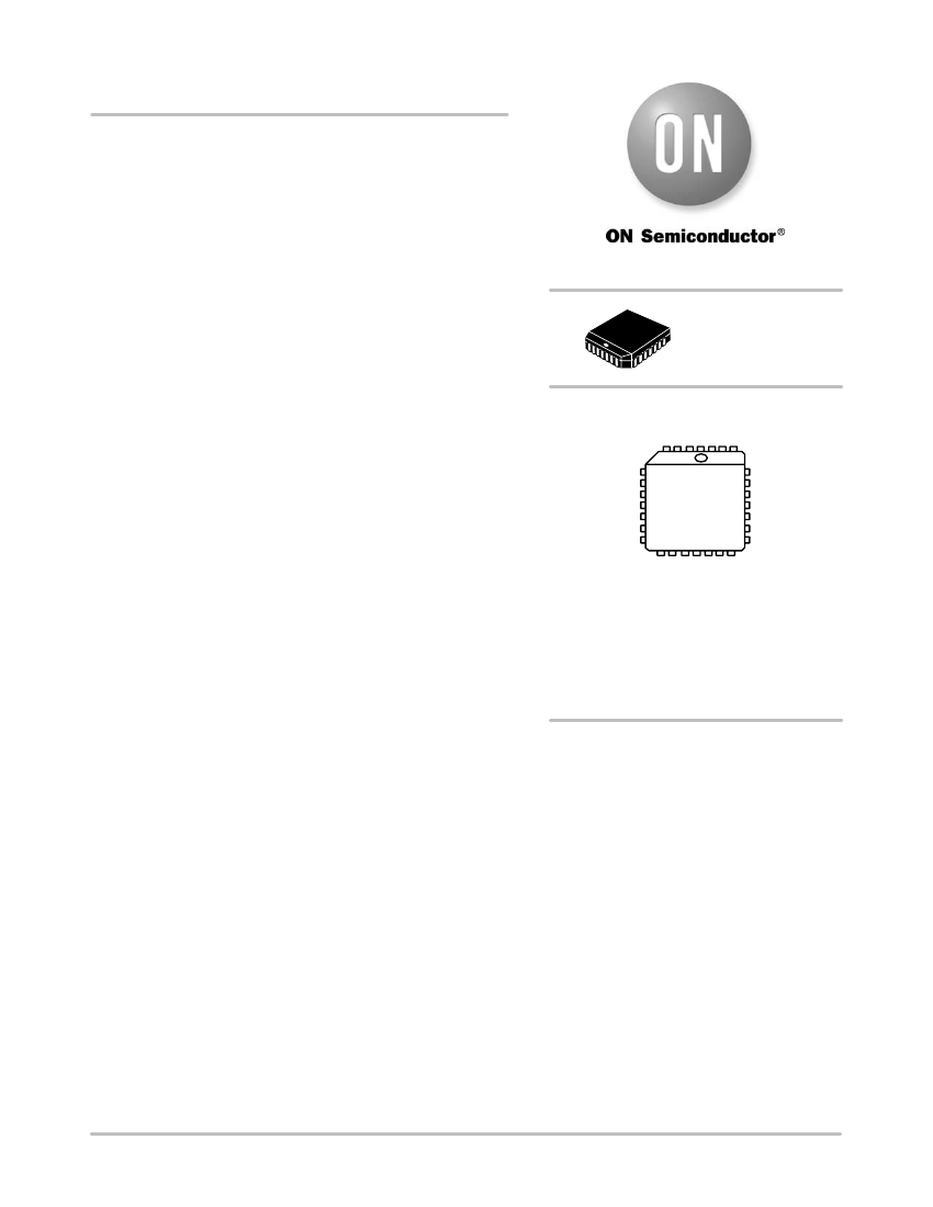
PLCC−28
FN SUFFIX
CASE 776
MARKING DIAGRAM*
1 28
MCxxxE446FNG
AWLYYWW
xxx
A
WL
YY
WW
G
= 10 or 100
= Assembly Location
= Wafer Lot
= Year
= Work Week
= Pb−Free Package
*For additional marking information, refer to
Application Note AND8002/D.
•
•
•
•
•
•
•
On Chip Clock
÷4
and
÷8
1.5 Gb/s Typical Data Rate Capability
Differential Clock and Serial Inputs
ORDERING INFORMATION
See detailed ordering and shipping information in the package
dimensions section on page 10 of this data sheet.
V
BB
Output for Single-ended Input Applications
Asynchronous Data Synchronization
Mode Select to Expand to 8 Bits
PECL Mode Operating Range: V
CC
= 4.2 V to 5.7 V
with V
EE
= 0 V
•
NECL Mode Operating Range: V
CC
= 0 V
with V
EE
=
−4.2
V to
−5.7
V
•
Internal Input 50 kW Pulldown Resistors
•
ESD Protection: Human Body Model; > 2 kV,
Machine Model; > 100 V
•
Meets or Exceeds JEDEC Spec EIA/JESD78 IC
•
•
•
•
Latchup Test
Flammability Rating: UL 94 V−0 @ 0.125 in,
Oxygen Index: 28 to 34
Transistor Count = 525 devices
Moisture Sensitivity Level: Pb = 1; Pb−Free = 3
For Additional Information, see Application Note
AND8003/D
Pb−Free Packages are Available*
*For additional information on our Pb−Free strategy and soldering details, please
download the ON Semiconductor Soldering and Mounting Techniques
Reference Manual, SOLDERRM/D.
©
Semiconductor Components Industries, LLC, 2006
November, 2006
−
Rev. 8
1
Publication Order Number:
MC10E446/D
MC10E446, MC100E446
Table 4. 10E SERIES PECL DC CHARACTERISTICS
V
CCx
= 5.0 V; V
EE
= 0.0 V (Note 1)
0°C
Symbol
I
EE
V
OH
VOH
SOUT
V
OL
V
IH
V
IL
V
BB
I
IH
I
IL
Characteristic
Power Supply Current
Output HIGH Voltage (Note 2)
Output HIGH Voltage
SOUT/SOUT
3980
3980
3050
3830
3050
3.62
3210
3995
3285
Min
Typ
126
4070
Max
151
4160
4210
3370
4160
3520
3.74
150
0.5
0.3
0.5
0.25
4020
4020
3050
3870
3050
3.65
3210
4030
3285
Min
25°C
Typ
126
4105
Max
151
4190
4240
3370
4190
3520
3.75
150
0.3
0.2
4090
4090
3050
3940
3050
3.69
3227
4110
3302
Min
85°C
Typ
126
4185
Max
151
4280
4330
3405
4280
3555
3.81
150
Unit
mA
mV
mV
mV
mV
mV
V
mA
mA
Output LOW Voltage (Note 2)
Input HIGH Voltage
Input LOW Voltage
Output Voltage Reference
Input HIGH Current
Input LOW Current
NOTE: Device will meet the specifications after thermal equilibrium has been established when mounted in a test socket or printed circuit
board with maintained transverse airflow greater than 500 lfpm. Electrical parameters are guaranteed only over the declared
operating temperature range. Functional operation of the device exceeding these conditions is not implied. Device specification limit
values are applied individually under normal operating conditions and not valid simultaneously.
1. Input and output parameters vary 1:1 with V
CC
. V
EE
can vary
−0.46
V / +0.06 V.
2. Outputs are terminated through a 50
W
resistor to V
CC
−
2.0 V.
Table 5. 10E SERIES NECL DC CHARACTERISTICS
V
CCx
= 0.0 V; V
EE
=
−5.0
V (Note 3)
0°C
Symbol
I
EE
V
OH
VOH
SOUT
V
OL
V
IH
V
IL
V
BB
I
IH
I
IL
Characteristic
Power Supply Current
Output HIGH Voltage (Note 4)
Output HIGH Voltage
SOUT/SOUT
−1020
−1020
−1950
−1170
−1950
−1.38
−1790
−1005
−1715
Min
Typ
126
−930
Max
151
−840
−790
−1630
−840
−1480
−1.27
150
0.5
0.3
0.5
0.065
−980
−980
−1950
−1130
−1950
−1.35
−1790
−970
−1715
Min
25°C
Typ
126
−895
Max
151
−810
−760
−1630
−810
−1480
−1.25
150
0.3
0.2
−910
−910
−1950
−1060
−1950
−1.31
−1773
−890
−1698
Min
85°C
Typ
126
−815
Max
151
−720
−670
−1595
−720
−1445
−1.19
150
Unit
mA
mV
mV
mV
mV
mV
V
mA
mA
Output LOW Voltage (Note 4)
Input HIGH Voltage
Input LOW Voltage
Output Voltage Reference
Input HIGH Current
Input LOW Current
NOTE: Device will meet the specifications after thermal equilibrium has been established when mounted in a test socket or printed circuit
board with maintained transverse airflow greater than 500 lfpm. Electrical parameters are guaranteed only over the declared
operating temperature range. Functional operation of the device exceeding these conditions is not implied. Device specification limit
values are applied individually under normal operating conditions and not valid simultaneously.
3. Input and output parameters vary 1:1 with V
CC
. V
EE
can vary
−0.46
V / +0.06 V.
4. Outputs are terminated through a 50
W
resistor to V
CC
−
2.0 V.
http://onsemi.com
5

 京公网安备 11010802033920号


