
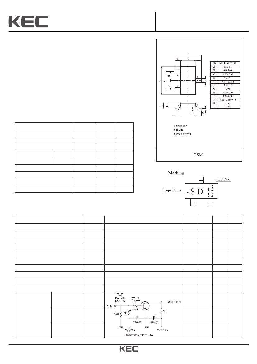
Small Signal Bipolar Transistor, 3A I(C), 20V V(BR)CEO, 1-Element, PNP, Silicon, ULTRASMALL, TSM, 3 PIN
| Parameter Name | Attribute value |
| Is it Rohs certified? | conform to |
| package instruction | SMALL OUTLINE, R-PDSO-G3 |
| Reach Compliance Code | unknown |
| ECCN code | EAR99 |
| Maximum collector current (IC) | 3 A |
| Collector-emitter maximum voltage | 20 V |
| Configuration | SINGLE |
| Minimum DC current gain (hFE) | 200 |
| JESD-30 code | R-PDSO-G3 |
| Number of components | 1 |
| Number of terminals | 3 |
| Package body material | PLASTIC/EPOXY |
| Package shape | RECTANGULAR |
| Package form | SMALL OUTLINE |
| Peak Reflow Temperature (Celsius) | NOT SPECIFIED |
| Polarity/channel type | PNP |
| surface mount | YES |
| Terminal form | GULL WING |
| Terminal location | DUAL |
| Maximum time at peak reflow temperature | NOT SPECIFIED |
| transistor applications | SWITCHING |
| Transistor component materials | SILICON |
| Nominal transition frequency (fT) | 160 MHz |
| Base Number Matches | 1 |
 京公网安备 11010802033920号


