Basic information of LM101AJG amplifier:
LM101AJG is an OPERATIONAL AMPLIFIER. The commonly used packaging method is DIP,
LM101AJG amplifier core information:
The minimum operating temperature of the LM101AJG is -55 °C and the maximum operating temperature is 125 °C. Its maximum average bias current is 0.075 µA
When the op amp is used in closed loop, at a certain closed-loop gain (usually 1 or 2, 10, etc.), the frequency when the LM101AJG gain becomes 0.707 times the low-frequency gain is 1000 kHz.
The nominal supply voltage of LM101AJG is 15 V, and its corresponding nominal negative supply voltage is -15 V. The input offset voltage of LM101AJG is 2000 µV (input offset voltage: the compensation voltage added between the two input terminals to make the output terminal of the operational amplifier 0V (or close to 0V).)
Related dimensions of LM101AJG:
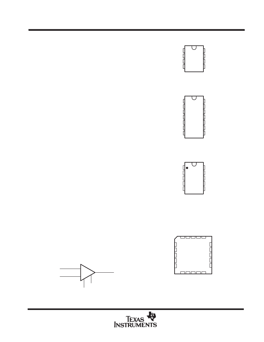
The width of LM101AJG is: 7.62 mm and the length is 9.6 mm. LM101AJG has 8 terminals. Its terminal position type is: DUAL. Terminal pitch is 2.54 mm.
LM101AJG amplifier additional information:
Its temperature grade is: MILITARY. The corresponding JESD-30 code is: R-GDIP-T8. The packaging code of LM101AJG is: DIP. The materials used in the LM101AJG package are mostly CERAMIC and GLASS-SEALED. The package shape is RECTANGULAR.
The LM101AJG package pin format is: IN-LINE. Its terminal form is: THROUGH-HOLE. The maximum seat height is 5.08 mm.
Basic information of LM101AJG amplifier:
LM101AJG is an OPERATIONAL AMPLIFIER. The commonly used packaging method is DIP,
LM101AJG amplifier core information:
The minimum operating temperature of the LM101AJG is -55 °C and the maximum operating temperature is 125 °C. Its maximum average bias current is 0.075 µA
When the op amp is used in closed loop, at a certain closed-loop gain (usually 1 or 2, 10, etc.), the frequency when the LM101AJG gain becomes 0.707 times the low-frequency gain is 1000 kHz.
The nominal supply voltage of LM101AJG is 15 V, and its corresponding nominal negative supply voltage is -15 V. The input offset voltage of LM101AJG is 2000 µV (input offset voltage: the compensation voltage added between the two input terminals to make the output terminal of the operational amplifier 0V (or close to 0V).)
Related dimensions of LM101AJG:
The width of LM101AJG is: 7.62 mm and the length is 9.6 mm. LM101AJG has 8 terminals. Its terminal position type is: DUAL. Terminal pitch is 2.54 mm.
LM101AJG amplifier additional information:
Its temperature grade is: MILITARY. The corresponding JESD-30 code is: R-GDIP-T8. The packaging code of LM101AJG is: DIP. The materials used in the LM101AJG package are mostly CERAMIC and GLASS-SEALED. The package shape is RECTANGULAR.
The LM101AJG package pin format is: IN-LINE. Its terminal form is: THROUGH-HOLE. The maximum seat height is 5.08 mm.
| Parameter Name | Attribute value |
| package instruction | DIP, |
| Reach Compliance Code | unknown |
| ECCN code | EAR99 |
| Amplifier type | OPERATIONAL AMPLIFIER |
| Maximum average bias current (IIB) | 0.075 µA |
| Nominal Common Mode Rejection Ratio | 98 dB |
| Maximum input offset voltage | 2000 µV |
| JESD-30 code | R-GDIP-T8 |
| length | 9.6 mm |
| Negative supply voltage upper limit | -22 V |
| Nominal Negative Supply Voltage (Vsup) | -15 V |
| Number of functions | 1 |
| Number of terminals | 8 |
| Maximum operating temperature | 125 °C |
| Minimum operating temperature | -55 °C |
| Package body material | CERAMIC, GLASS-SEALED |
| encapsulated code | DIP |
| Package shape | RECTANGULAR |
| Package form | IN-LINE |
| Maximum seat height | 5.08 mm |
| Supply voltage upper limit | 22 V |
| Nominal supply voltage (Vsup) | 15 V |
| surface mount | NO |
| technology | BIPOLAR |
| Temperature level | MILITARY |
| Terminal form | THROUGH-HOLE |
| Terminal pitch | 2.54 mm |
| Terminal location | DUAL |
| Nominal Uniform Gain Bandwidth | 1000 kHz |
| width | 7.62 mm |
| Base Number Matches | 1 |
| LM101AJG | LM101AD | LM101AP | LM101AU | LM101AW | LM301AP | |
|---|---|---|---|---|---|---|
| Description | Operational Amplifier, 1 Func, 2000uV Offset-Max, BIPolar, CDIP8, HERMETIC SEALED, CERAMIC, DIP-8 | Operational Amplifier, 1 Func, 2000uV Offset-Max, PDSO8, SOIC-8 | Operational Amplifier, 1 Func, 2000uV Offset-Max, PDIP8, PLASTIC, DIP-8 | Operational Amplifier, 1 Func, 2000uV Offset-Max, BIPolar, CDFP10, HERMETIC SEALED, CERAMIC, FP-10 | Operational Amplifier, 1 Func, 2000uV Offset-Max, BIPolar, CDFP14, HERMETIC SEALED, CERAMIC, FP-14 | Operational Amplifier, 1 Func, 7500uV Offset-Max, BIPolar, PDIP8, PLASTIC, DIP-8 |
| package instruction | DIP, | SOP, | DIP, | DFP, | DFP, | DIP, |
| Reach Compliance Code | unknown | unknown | unknown | unknown | unknown | unknown |
| ECCN code | EAR99 | EAR99 | EAR99 | EAR99 | EAR99 | EAR99 |
| Amplifier type | OPERATIONAL AMPLIFIER | OPERATIONAL AMPLIFIER | OPERATIONAL AMPLIFIER | OPERATIONAL AMPLIFIER | OPERATIONAL AMPLIFIER | OPERATIONAL AMPLIFIER |
| Maximum average bias current (IIB) | 0.075 µA | 0.075 µA | 0.075 µA | 0.075 µA | 0.075 µA | 0.25 µA |
| Nominal Common Mode Rejection Ratio | 98 dB | 98 dB | 98 dB | 98 dB | 98 dB | 90 dB |
| Maximum input offset voltage | 2000 µV | 2000 µV | 2000 µV | 2000 µV | 2000 µV | 7500 µV |
| JESD-30 code | R-GDIP-T8 | R-PDSO-G8 | R-PDIP-T8 | R-GDFP-F10 | R-GDFP-F14 | R-PDIP-T8 |
| length | 9.6 mm | 4.9 mm | 9.81 mm | 6.35 mm | 8.725 mm | 9.81 mm |
| Negative supply voltage upper limit | -22 V | -22 V | -22 V | -22 V | -22 V | -18 V |
| Nominal Negative Supply Voltage (Vsup) | -15 V | -15 V | -15 V | -15 V | -15 V | -15 V |
| Number of functions | 1 | 1 | 1 | 1 | 1 | 1 |
| Number of terminals | 8 | 8 | 8 | 10 | 14 | 8 |
| Maximum operating temperature | 125 °C | 125 °C | 125 °C | 125 °C | 125 °C | 70 °C |
| Minimum operating temperature | -55 °C | -55 °C | -55 °C | -55 °C | -55 °C | - |
| Package body material | CERAMIC, GLASS-SEALED | PLASTIC/EPOXY | PLASTIC/EPOXY | CERAMIC, GLASS-SEALED | CERAMIC, GLASS-SEALED | PLASTIC/EPOXY |
| encapsulated code | DIP | SOP | DIP | DFP | DFP | DIP |
| Package shape | RECTANGULAR | RECTANGULAR | RECTANGULAR | RECTANGULAR | RECTANGULAR | RECTANGULAR |
| Package form | IN-LINE | SMALL OUTLINE | IN-LINE | FLATPACK | FLATPACK | IN-LINE |
| Maximum seat height | 5.08 mm | 1.75 mm | 5.08 mm | 2.03 mm | 2.03 mm | 5.08 mm |
| Supply voltage upper limit | 22 V | 22 V | 22 V | 22 V | 22 V | 18 V |
| Nominal supply voltage (Vsup) | 15 V | 15 V | 15 V | 15 V | 15 V | 15 V |
| surface mount | NO | YES | NO | YES | YES | NO |
| Temperature level | MILITARY | MILITARY | MILITARY | MILITARY | MILITARY | COMMERCIAL |
| Terminal form | THROUGH-HOLE | GULL WING | THROUGH-HOLE | FLAT | FLAT | THROUGH-HOLE |
| Terminal pitch | 2.54 mm | 1.27 mm | 2.54 mm | 1.27 mm | 1.27 mm | 2.54 mm |
| Terminal location | DUAL | DUAL | DUAL | DUAL | DUAL | DUAL |
| width | 7.62 mm | 3.9 mm | 7.62 mm | 6.16 mm | 6.35 mm | 7.62 mm |
| technology | BIPOLAR | - | - | BIPOLAR | BIPOLAR | BIPOLAR |
| Nominal Uniform Gain Bandwidth | 1000 kHz | - | - | 1000 kHz | 1000 kHz | 1000 kHz |
| Base Number Matches | 1 | 1 | 1 | 1 | - | - |
| Maker | - | Rochester Electronics | Rochester Electronics | Rochester Electronics | Rochester Electronics | Rochester Electronics |
 京公网安备 11010802033920号


