LM101A, LM201A, LM301A
HIGH-PERFORMANCE OPERATIONAL AMPLIFIERS
D961, OCTOBER 1979 – REVISED SEPTEMBER 1990
•
•
•
•
•
•
•
•
•
Low Input Currents
Low Input Offset Parameters
Frequency and Transient Response
Characteristics Adjustable
Short-Circuit Protection
Offset-Voltage Null Capability
No Latch-Up
Wide Common-Mode and Differential
Voltage Ranges
Same Pin Assignments as uA709
Designed to be Interchangeable with
National Semiconductor LM101A and
LM301A
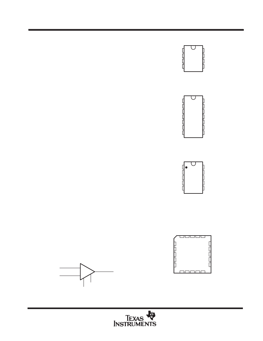
D, JG, OR P PACKAGE
(T0P VIEW)
N1/COMP
IN –
IN +
V
CC–
1
2
3
4
8
7
6
5
COMP
V
CC+
OUT
OFFSET N2
LM101A
W FLAT PACKAGE
(T0P VIEW)
description
The LM101A, LM201A, and LM301A are high-
performance operational amplifiers featuring very
low input bias current and input offset voltage and
current to improve the accuracy of high-
impedance circuits using these devices. The high
common-mode input voltage range and the
absence of latch-up make these amplifiers ideal
for voltage-follower applications. The devices are
protected to withstand short circuits at the output.
The external compensation of these amplifiers
allows the changing of the frequency response
(when the closed-loop gain is greater then unity)
for applications requiring wider bandwidth or
higher slew rate. A potentiometer may be
connected between the offset-null inputs (N1 and
N2), as shown in Figure 7, to null out the offset
voltage.
The LM101A is characterized for operation over
the full military temperature range of – 55°C to
125°C, the LM201A is characterized for operation
from – 25°C to 85°C, and the LM301A is
characterized for operation from 0°C to 70°C.
NC
NC
N1/COMP
IN –
IN +
V
CC –
NC
1
2
3
4
5
6
7
14
13
12
11
10
9
8
NC
NC
COMP
V
CC+
OUT
OFFSET N2
NC
LM101A
U FLAT PACKAGE
(T0P VIEW)
NC
N1/COMP
IN –
IN +
V
CC –
1
2
3
4
5
10
9
8
7
6
NC
COMP
V
CC+
OUT
OFFSET N2
LM101A
FK CHIP-CARRIER PACKAGE
(T0P VIEW)
symbol
Noninverting
Input IN+
Inverting
Input IN–
+
Output
–
N2
N1/
COMP
NC
IN –
NC
IN +
NC
4
5
6
7
8
3 2 1 20 19
18
17
16
15
14
9 10 11 12 13
NC
N1/COMP
NC
COMP
NC
NC
V
CC+
NC
OUT
NC
NC – No internal connection
Copyright
©
1991, Texas Instruments Incorporated
PRODUCTION DATA information is current as of publication date.
Products conform to specifications per the terms of Texas Instruments
standard warranty. Production processing does not necessarily include
testing of all parameters.
POST OFFICE BOX 655303
•
DALLAS, TEXAS 75265
V
CC –
NC
N2
NC
NC
2–1
LM101A, LM201A, LM301A
HIGH-PERFORMANCE OPERATIONAL AMPLIFIERS
AVAILABLE OPTIONS
PACKAGE
TA
VIO MAX
at 25°C
SMALL OUTLINE
(D)
0°C to 70°C
– 25
°C
to 85°C
– 55
°C
to 125°C
7.5 mV
2 mV
2 mV
LM301AD
LM201AD
LM101AD
CHIP CARRIER
(FK)
–
–
LM101AFK
CERAMIC DIP
(JG)
–
–
LM101AJG
PLASTIC DIP
(P)
LM301AP
LM201AP
LM101AP
FLAT
PACK
(U)
–
–
LM101AU
FLAT PACK
(W)
–
–
LM101AW
The D package is available taped and reeled. Add the suffix R to the device type, (i.e., LM301ADR).
absolute maximum ratings over operating free-air temperature range (unless otherwise noted)
LM101A
Supply voltage VCC+ (see Note 1)
Supply voltage VCC– (see Note 1)
Differential input voltage (see Note 2)
Input voltage (either input, see Notes 1 and 3)
Voltage between either offset null terminal (N1/N2) and VCC–
Duration of output short-circuit (see Note 4)
Continuous total power dissipation
Operating free-air temperature range
Storage temperature range
Case temperature for 60 seconds: FK package
Lead temperature 1,6 mm (1/16 inch) from case for 60 seconds
Lead temperature 1,6 mm (1/16 inch) from case for 10 seconds
NOTES: 1.
2.
3.
4.
JG, U, or W package
D or P package
22
– 22
±30
±15
– 0.5 to 2
unlimited
– 55 to 125
– 65 to 150
260
300
260
260
260
LM201A
22
– 22
±30
±15
– 0.5 to 2
unlimited
– 25 to 85
– 65 to 150
LM301A
18
– 18
±30
±15
– 0.5 to 2
unlimited
0 to 70
– 65 to 150
°C
°C
°C
°C
°C
UNIT
V
V
V
V
V
See Dissipation Rating Table
All voltage values, unless otherwise noted, are with respect to the midpoint between VCC+ and VCC–.
Differential voltages are at the noninverting input terminal with respect to the inverting input terminal.
The magnitude of the input voltage must never exceed the magnitude of the supply voltage or 15 V, whichever is less.
The output may be shorted to ground or either power supply. For the LM101A only, the unlimited duration of the short-circuit applies
at (or above) 125°C case temperature or 75°C free-air temperature. For the LM201A only, the unlimited duration of the short-circuit
applies at (or below) 85°C case temperatuare or 75°C free-air temperature.
DISSIPATION RATING TABLE
PACKAGE
TA
≤
25°C
POWER RATING
500 mW
500 mW
500 mW
500 mW
500 mW
500 mW
DERATING
FACTOR
5.8 mW/°C
11.0 mW/°C
8.4 mW/°C
8.0 mW/°C
5.4 mW/°C
8.0 mW/°C
DERATE
ABOVE TA
64°C
105°C
90°C
87°C
57°C
87°C
TA = 70°C
POWER RATING
464 mW
500 mW
500 mW
500 mW
432 mW
500 mW
TA = 85°C
POWER RATING
377 mW
500 mW
500 mW
500 mW
351 mW
500 mW
TA = 125°C
POWER RATING
145 mW
275 mW
210 mW
200 mW
135 mW
200 mW
D
FK
JG
P
U
W
recommended operating conditions
MIN
Supply voltage, VCC+
Supply voltage, VCC–
5
–
5
MAX
18
–
18
UNIT
V
2–2
POST OFFICE BOX 655303
•
DALLAS, TEXAS 75265
LM101A, LM201A, LM301A
HIGH-PERFORMANCE OPERATIONAL AMPLIFIERS
electrical characteristics at specified free-air temperature, C
C
= 30 pF (see Note 5)
PARAMETER
VIO
α
VIO
IIO
Input offset voltage
Average temperature coefficient of
input offset voltage
Input offset current
TEST CONDITIONS†
VO = 0
VO = 0
25°C
Full range
Full range
25°C
Full range
TA = – 55°C to 25°C
TA = 25°C to MAX
TA = 0°C to 25°C
TA = 25°C to 70°C
25°C
Full range
See Note 6
VCC± =
±15
V,
RL = 10 kΩ
VCC± =
±15
V,
RL = 2 kΩ
VCC± =
±15
V,
VO =
±10
V,
RL
≥
2 kΩ
Full range
25°C
Full range
25°C
Full range
25°C
Full range
25°C
VIC = VICR min
25°C
Full range
25°C
Full range
No load, VO = 0,
See Note 6
25°C
MAX
±15
24
24
20
20
50
25
1.5
80
80
80
80
1.8
1.2
3
2.5
98
4
98
200
26
28
30
75
100
±12
24
24
20
20
25
15
0.5
70
70
70
70
1.8
3
96
2
90
dB
dB
mA
200
V/mV
MΩ
26
28
V
0.02
0.01
3
1.5
LM101A, LM201A
MIN
TYP
0.6
MAX
2
3
15
10
20
0.2
0.1
0.02
0.01
70
0.6
0.3
250
300
nA
V
nA/°C
6
3
MIN
LM301A
TYP
2
MAX
7.5
10
30
50
70
nA
UNIT
mV
µV/°C
α
IIO
Average temperature coefficient of
input offset current
IIB
VICR
Input bias current
Common-mode input voltage range
Maximum peak-to-peak output
voltage swing
VOPP
AVD
ri
CMRR
kSVR
ICC
Large-signal differential voltage
amplification
Input resistance
Common-mode rejection ratio
Supply voltage rejection ratio
(∆ VCC/∆ VIO)
Supply current
† All characteristics are measured under open-loop conditions with zero common-mode input voltage unless otherwise specified. Full range for
LM101A is – 55°C to 125°C, for LM201A is – 25°C to 85°C, and for LM301A is 0°C to 70°C.
NOTES: 5. Unless otherwise noted, VCC± =
±
5 V to
±
20 V for LM101A and LM201A, and VCC± =
±
5 V to
±
15 V for LM301A. All typical values
are at VCC± =
±15
V.
6. For LM101A and LM201A, VCC± =
±
20 V. For LM301A, VCC± =
±
15 V.
POST OFFICE BOX 655303
•
DALLAS, TEXAS 75265
2–3
LM101A, LM201A, LM301A
HIGH-PERFORMANCE OPERATIONAL AMPLIFIERS
TYPICAL CHARACTERISTICS
INPUT OFFSET CURRENT
vs
FREE-AIR TEMPERATURE
4
VCC
±
=
±15
V
I IB – Input Bias Current – nA
I IO – Input Offset Current – nA
80
LM301A
60
100
VCC
±
=
±15
V
INPUT BIAS CURRENT
vs
FREE-AIR TEMPERATURE
3
LM301A
2I
40
1
LM101A
LM201A
20
LM101A
LM201A
0
–7
–50
–25
0
25
50
75 100
TA – Free-Air Temperature –
°C
125
0
–75
–50
–25
0
25
50
75
100
TA – Free-Air Temperature –
°C
125
Figure 1
MAXIMUM PEAK-TO-PEAK OUTPUT
VOLTAGE
(WITH SINGLE-POLE COMPENSATION)
vs
FREQUENCY
A VD – Differential Voltage Amplification – V/mV
VCC
±
=
±15
V
RL = 10 KΩ
TA = 25°C
Figure 2
OPEN-LOOP LARGE-SIGNAL DIFFERENTIAL
VOLTAGE AMPLIFICATION
vs
SUPPLY VOLTAGE
400
RL = 2 KΩ
TA = 25°C
200
VOPP – Maximum Peak-to-Peak Output Voltage – V
30
28
24
20
16
12
100
40
CC = 3 pF
8
CC = 30 pF
4
0
1k
LM301A
LM101A
LM201A
20
10 k
100 k
f – Frequency – Hz
1M
10 M
10
0
2
4
8 10 12 14 16
| VCC± | – Supply Voltage – V
6
18 20
Figure 3
Figure 4
2–4
POST OFFICE BOX 655303
•
DALLAS, TEXAS 75265
LM101A, LM201A, LM301A
HIGH-PERFORMANCE OPERATIONAL AMPLIFIERS
TYPICAL CHARACTERISTICS
OPEN-LOOP LARGE-SIGNAL DIFFERENTIAL
VOLTAGE AMPLIFICATION
vs
FREQUENCY
107
A VD – Differential Voltage Amplification
106
105
104
103
102
101
1
10–1
VCC
±
=
±15
V
RL = 2 kΩ
CC = 30 pF
TA = 25°C
8
6
Input and Output Voltages – V
4
2
Output
0
–2
Input
–4
–6
–8
1
10
100
1k
10 k 100 k 1 M
10 M 100 M
f – Frequency – Hz
VCC
±
=
±15
V
RL = 2 kΩ
CL = 100 pF
CC = 30 pF
TA = 25°C
VOLTAGE-FOLLOWER
LARGE-SIGNAL PULSE RESPONSE
0
10
20
30 40 50
t – Time –
µs
60
70
80
90
Figure 5
Figure 6
TYPICAL APPLICATION DATA
R2
VCC+
V
O
V
I
C
C
+ *
R2
R1
30 pF
w
R1
@)
R2
R1
R1
@
+
R1
)
R2
R2
R1
–
R3
+
VO
RL
≥
2 kΩ
VI
R3
VCC–
COMP
N1
5 MΩ
CC
N2
5.1 MΩ
Figure 7. Inverting Circuit with Adjustable Gain, Single-Pole Compensation,
and Offset Adjustment
POST OFFICE BOX 655303
•
DALLAS, TEXAS 75265
2–5
 京公网安备 11010802033920号


