HA4P5033-5 amplifier basic information:
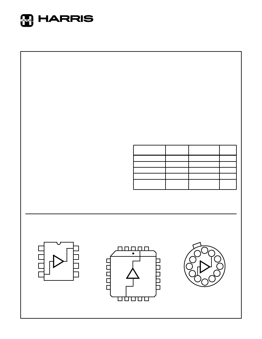
HA4P5033-5 is a BUFFER. Commonly used packaging methods are QCCJ, LDCC20,.4SQ
HA4P5033-5 amplifier core information:
The minimum operating temperature of the HA4P5033-5 is 75 °C. Maximum bias current at 25°C: 35 µA Maximum average bias current is 50 µA
How to simply check the efficiency of an amplifier? Looking at its slew rate, the HA4P5033-5 has a nominal slew rate of 0.0011 V/us. The maximum slew rate of the HA4P5033-5 given by the manufacturer is 30 mA, while the minimum slew rate is 1000 V/us. When the op amp is used in closed loop, at a certain closed-loop gain (usually 1 or 2, 10, etc.), the frequency when the HA4P5033-5 gain becomes 0.707 times the low-frequency gain is 250 MHz.
The nominal supply voltage of the HA4P5033-5 is 12 V, and its corresponding nominal negative supply voltage is -12 V. The input offset voltage of HA4P5033-5 is 25000 µV (input offset voltage: the compensation voltage added between the two input terminals to make the output terminal of the operational amplifier 0V (or close to 0V).)
Related dimensions of HA4P5033-5:
HA4P5033-5 has 20 terminals. Its terminal position type is: QUAD. Terminal pitch is 1.27 mm.
HA4P5033-5 amplifier additional information:
Its temperature grade is: COMMERCIAL EXTENDED. HA4P5033-5 is not Rohs certified. The corresponding JESD-30 code is: S-PQCC-J20. The corresponding JESD-609 code is: e0. The packaging code of HA4P5033-5 is: QCCJ.
HA4P5033-5 packaging materials are mostly PLASTIC/EPOXY. The package shape is SQUARE. The HA4P5033-5 package pin format is: CHIP CARRIER. Its terminal form is: J BEND.
HA4P5033-5 amplifier basic information:
HA4P5033-5 is a BUFFER. Commonly used packaging methods are QCCJ, LDCC20,.4SQ
HA4P5033-5 amplifier core information:
The minimum operating temperature of the HA4P5033-5 is 75 °C. Maximum bias current at 25°C: 35 µA Maximum average bias current is 50 µA
How to simply check the efficiency of an amplifier? Looking at its slew rate, the HA4P5033-5 has a nominal slew rate of 0.0011 V/us. The maximum slew rate of the HA4P5033-5 given by the manufacturer is 30 mA, while the minimum slew rate is 1000 V/us. When the op amp is used in closed loop, at a certain closed-loop gain (usually 1 or 2, 10, etc.), the frequency when the HA4P5033-5 gain becomes 0.707 times the low-frequency gain is 250 MHz.
The nominal supply voltage of the HA4P5033-5 is 12 V, and its corresponding nominal negative supply voltage is -12 V. The input offset voltage of HA4P5033-5 is 25000 µV (input offset voltage: the compensation voltage added between the two input terminals to make the output terminal of the operational amplifier 0V (or close to 0V).)
Related dimensions of HA4P5033-5:
HA4P5033-5 has 20 terminals. Its terminal position type is: QUAD. Terminal pitch is 1.27 mm.
HA4P5033-5 amplifier additional information:
Its temperature grade is: COMMERCIAL EXTENDED. HA4P5033-5 is not Rohs certified. The corresponding JESD-30 code is: S-PQCC-J20. The corresponding JESD-609 code is: e0. The packaging code of HA4P5033-5 is: QCCJ.
HA4P5033-5 packaging materials are mostly PLASTIC/EPOXY. The package shape is SQUARE. The HA4P5033-5 package pin format is: CHIP CARRIER. Its terminal form is: J BEND.
| Parameter Name | Attribute value |
| Is it Rohs certified? | incompatible |
| package instruction | QCCJ, LDCC20,.4SQ |
| Reach Compliance Code | unknown |
| ECCN code | EAR99 |
| Amplifier type | BUFFER |
| Maximum average bias current (IIB) | 50 µA |
| Nominal bandwidth (3dB) | 250 MHz |
| Maximum bias current (IIB) at 25C | 35 µA |
| Maximum input offset voltage | 25000 µV |
| JESD-30 code | S-PQCC-J20 |
| JESD-609 code | e0 |
| Negative supply voltage upper limit | -20 V |
| Nominal Negative Supply Voltage (Vsup) | -12 V |
| Number of functions | 1 |
| Number of terminals | 20 |
| Maximum operating temperature | 75 °C |
| Minimum operating temperature | |
| Minimum output current | 0.08 A |
| Package body material | PLASTIC/EPOXY |
| encapsulated code | QCCJ |
| Encapsulate equivalent code | LDCC20,.4SQ |
| Package shape | SQUARE |
| Package form | CHIP CARRIER |
| power supply | +-12 V |
| Certification status | Not Qualified |
| minimum slew rate | 1000 V/us |
| Nominal slew rate | 0.0011 V/us |
| Maximum slew rate | 30 mA |
| Supply voltage upper limit | 20 V |
| Nominal supply voltage (Vsup) | 12 V |
| surface mount | YES |
| technology | BIPOLAR |
| Temperature level | COMMERCIAL EXTENDED |
| Terminal surface | Tin/Lead (Sn/Pb) |
| Terminal form | J BEND |
| Terminal pitch | 1.27 mm |
| Terminal location | QUAD |
| Base Number Matches | 1 |
| HA4P5033-5 | HA2-5033-2 | HA2-5033-5 | HA9P5033-5 | |
|---|---|---|---|---|
| Description | Buffer Amplifier, 1 Func, BIPolar, PQCC20 | Buffer Amplifier, 1 Func, BIPolar, MBCY12 | Buffer Amplifier, 1 Func, BIPolar, MBCY12 | Buffer Amplifier, 1 Func, BIPolar, PDSO8 |
| Is it Rohs certified? | incompatible | incompatible | incompatible | incompatible |
| package instruction | QCCJ, LDCC20,.4SQ | QIP, QUAD12,.4SQ | QIP, QUAD12,.4SQ | SOP, SOP8,.25 |
| Reach Compliance Code | unknown | unknown | unknown | unknown |
| ECCN code | EAR99 | EAR99 | EAR99 | EAR99 |
| Amplifier type | BUFFER | BUFFER | BUFFER | BUFFER |
| Maximum average bias current (IIB) | 50 µA | 50 µA | 50 µA | 50 µA |
| Nominal bandwidth (3dB) | 250 MHz | 250 MHz | 250 MHz | 250 MHz |
| Maximum bias current (IIB) at 25C | 35 µA | 35 µA | 35 µA | 35 µA |
| Maximum input offset voltage | 25000 µV | 25000 µV | 25000 µV | 25000 µV |
| JESD-30 code | S-PQCC-J20 | O-MBCY-W12 | O-MBCY-W12 | R-PDSO-G8 |
| JESD-609 code | e0 | e0 | e0 | e0 |
| Negative supply voltage upper limit | -20 V | -20 V | -20 V | -20 V |
| Nominal Negative Supply Voltage (Vsup) | -12 V | -12 V | -12 V | -12 V |
| Number of functions | 1 | 1 | 1 | 1 |
| Number of terminals | 20 | 12 | 12 | 8 |
| Maximum operating temperature | 75 °C | 125 °C | 75 °C | 60 °C |
| Minimum output current | 0.08 A | 0.08 A | 0.08 A | 0.08 A |
| Package body material | PLASTIC/EPOXY | METAL | METAL | PLASTIC/EPOXY |
| encapsulated code | QCCJ | QIP | QIP | SOP |
| Encapsulate equivalent code | LDCC20,.4SQ | QUAD12,.4SQ | QUAD12,.4SQ | SOP8,.25 |
| Package shape | SQUARE | ROUND | ROUND | RECTANGULAR |
| Package form | CHIP CARRIER | CYLINDRICAL | CYLINDRICAL | SMALL OUTLINE |
| power supply | +-12 V | +-12 V | +-12 V | +-12 V |
| Certification status | Not Qualified | Not Qualified | Not Qualified | Not Qualified |
| minimum slew rate | 1000 V/us | 1000 V/us | 1000 V/us | 1000 V/us |
| Nominal slew rate | 0.0011 V/us | 1100 V/us | 1100 V/us | 1100 V/us |
| Maximum slew rate | 30 mA | 30 mA | 30 mA | 30 mA |
| Supply voltage upper limit | 20 V | 20 V | 20 V | 20 V |
| Nominal supply voltage (Vsup) | 12 V | 12 V | 12 V | 12 V |
| surface mount | YES | NO | NO | YES |
| technology | BIPOLAR | BIPOLAR | BIPOLAR | BIPOLAR |
| Temperature level | COMMERCIAL EXTENDED | MILITARY | COMMERCIAL EXTENDED | OTHER |
| Terminal surface | Tin/Lead (Sn/Pb) | Tin/Lead (Sn/Pb) | Tin/Lead (Sn/Pb) | Tin/Lead (Sn/Pb) |
| Terminal form | J BEND | WIRE | WIRE | GULL WING |
| Terminal pitch | 1.27 mm | 2.54 mm | 2.54 mm | 1.27 mm |
| Terminal location | QUAD | BOTTOM | BOTTOM | DUAL |
| Base Number Matches | 1 | 1 | 1 | 1 |
 京公网安备 11010802033920号


