
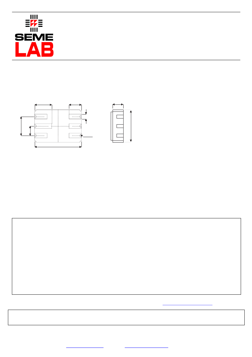
Small Signal Bipolar Transistor, 0.2A I(C), 60V V(BR)CEO, 2-Element, NPN and PNP, Silicon, MO-041BB, HERMETIC SEALED, CERAMIC, LCC2-6
| Parameter Name | Attribute value |
| Is it Rohs certified? | conform to |
| package instruction | SMALL OUTLINE, R-CDSO-N6 |
| Reach Compliance Code | compliant |
| ECCN code | EAR99 |
| Maximum collector current (IC) | 0.2 A |
| Collector-emitter maximum voltage | 60 V |
| Configuration | SEPARATE, 2 ELEMENTS |
| Minimum DC current gain (hFE) | 160 |
| JEDEC-95 code | MO-041BB |
| JESD-30 code | R-CDSO-N6 |
| JESD-609 code | e4 |
| Number of components | 2 |
| Number of terminals | 6 |
| Package body material | CERAMIC, METAL-SEALED COFIRED |
| Package shape | RECTANGULAR |
| Package form | SMALL OUTLINE |
| Peak Reflow Temperature (Celsius) | NOT SPECIFIED |
| Polarity/channel type | NPN AND PNP |
| Certification status | Not Qualified |
| surface mount | YES |
| Terminal surface | GOLD |
| Terminal form | NO LEAD |
| Terminal location | DUAL |
| Maximum time at peak reflow temperature | NOT SPECIFIED |
| Transistor component materials | SILICON |
| Nominal transition frequency (fT) | 40 MHz |
| Base Number Matches | 1 |
 京公网安备 11010802033920号


