NPN BDY53 – BDY54
SILICON TRANSISTORS, DIFFUSED MESA
They are mounted in TO-3 metal package.
LF Large Signal Power Amplification
High Current Fast Switching
Compliance to RoHS.
ABSOLUTE MAXIMUM RATINGS
Symbol
V
CEO
V
CBO
V
EBO
I
C
I
B
P
TOT
Collector-Emitter Voltage
Collector-Base Voltage
Emitter-Base Voltage
Collector Current
Base Current
Power Dissipation
Junction Temperature
T
J
Ratings
BDY53
BDY54
BDY53
BDY54
Value
60
120
100
180
7
12
5
Unit
V
V
V
A
A
W
@ T
C
= 25°
60
-65 to +200
T
S
Storage Temperature
°C
08/11/2012
COMSET SEMICONDUCTORS
1|3
NPN BDY53 – BDY54
ELECTRICAL CHARACTERISTICS
TC=25°C unless otherwise noted
Symbol
V
CEO(SUS)
I
EBO
Ratings
Collector-Emitter
Breakdown Voltage (*)
Emitter-Base Cutoff
Current
Collector-Emitter Cutoff
Current
Test Condition(s)
I
C
=100 mA, I
B
=0
V
EB
=7 V
V
CE
=100 V
V
BE
=-1.5 V
T
CASE
=150°C
V
CE
=150 V
V
BE
=-1.5 V
T
CASE
=150°C
BDY53
BDY54
BDY53
BDY54
BDY53
Min
60
120
-
-
Typ
-
-
-
-
Max
-
-
3.0
Unit
V
mA
I
CEX
15
BDY54
-
-
-
-
-
20
20
-
-
-
-
-
-
-
-
-
0.3
1.8
1.1
mA
V
CE(SAT)
Collector-Emitter saturation I
C
=4.0 A, I
B
=0.4 A
Voltage (*)
I
C
=7.0 A, I
B
=1.4 A
V
BE(SAT)
Base-Emitter Voltage (*)
Static Forward Current
transfer ratio (*)
Transition Frequency
Turn-on time
Turn-off time
h
21E
f
T
t
d
+ t
r
t
s
+ t
f
BDY53
BDY54
BDY53
BDY54
BDY53
I
C
=4.0 A, I
B
=0.4 A
BDY54
BDY53
I
C
=7.0 A, I
B
=1.4 A
BDY54
BDY53
V
CE
=1.5 V, I
C
=2 A
BDY54
V
CE
=4.0 V, I
C
=0.5 A BDY53
f=10 MHz
BDY54
BDY53
I
C
=5 A, I
B
=1 A
BDY54
I
C
=5 A
BDY53
I
B1
=1 A
BDY54
I
B2
=-0.5 A
V
2.2
2
V
2.5
60
-
-
-
V
MHz
µs
µs
(*) Pulse Width
≈
300
µs,
Duty Cycle
∠
2.0%
08/11/2012
COMSET SEMICONDUCTORS
2|3
NPN BDY53 – BDY54
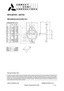
MECHANICAL DATA CASE TO-3
DIMENSIONS (mm)
min
A
B
C
D
F
G
N
P
R
U
V
11
0.97
1.5
8.32
19
10.70
16.50
25
4
38.50
30
max
13.10
1.15
1.65
8.92
20
11.1
17.20
26
4.09
39.30
30.30
Pin 1 :
Pin 2 :
Case :
Base
Emitter
Collector
Revised October 2012
Information furnished is believed to be accurate and reliable. However, Comset Semiconductors assumes no responsibility for the consequences of
use of such information nor for any infringement of patents or other rights of third parties which may results from its use. Data are subject to change
without notice. Comset Semiconductors makes no warranty, representation or guarantee regarding the suitability of its products for any particular
purpose, nor does Comset Semiconductors assume any liability arising out of the application or use of any product and specifically disclaims any
and all liability, including without limitation consequential or incidental damages. Comset Semiconductors’ products are not authorized for use as
critical components in life support devices or systems.
www.comsetsemi.com
08/11/2012
COMSET SEMICONDUCTORS
info@comsetsemi.com
3|3

 京公网安备 11010802033920号