
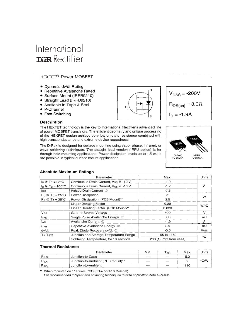
Power Field-Effect Transistor, 1.9A I(D), 200V, 3ohm, 1-Element, P-Channel, Silicon, Metal-oxide Semiconductor FET, TO-252AA, LEAD FREE, DPAK-3
| Parameter Name | Attribute value |
| Is it lead-free? | Lead free |
| Is it Rohs certified? | conform to |
| Maker | International Rectifier ( Infineon ) |
| Parts packaging code | TO-252AA |
| package instruction | LEAD FREE, DPAK-3 |
| Contacts | 3 |
| Reach Compliance Code | not_compliant |
| ECCN code | EAR99 |
| Other features | AVALANCHE RATED |
| Avalanche Energy Efficiency Rating (Eas) | 300 mJ |
| Shell connection | DRAIN |
| Configuration | SINGLE WITH BUILT-IN DIODE |
| Minimum drain-source breakdown voltage | 200 V |
| Maximum drain current (ID) | 1.9 A |
| Maximum drain-source on-resistance | 3 Ω |
| FET technology | METAL-OXIDE SEMICONDUCTOR |
| JEDEC-95 code | TO-252AA |
| JESD-30 code | R-PSSO-G2 |
| JESD-609 code | e3 |
| Humidity sensitivity level | 1 |
| Number of components | 1 |
| Number of terminals | 2 |
| Operating mode | ENHANCEMENT MODE |
| Package body material | PLASTIC/EPOXY |
| Package shape | RECTANGULAR |
| Package form | SMALL OUTLINE |
| Peak Reflow Temperature (Celsius) | 260 |
| Polarity/channel type | P-CHANNEL |
| Maximum pulsed drain current (IDM) | 7.6 A |
| Certification status | Not Qualified |
| surface mount | YES |
| Terminal surface | MATTE TIN OVER NICKEL |
| Terminal form | GULL WING |
| Terminal location | SINGLE |
| Maximum time at peak reflow temperature | 30 |
| transistor applications | SWITCHING |
| Transistor component materials | SILICON |
| Base Number Matches | 1 |
| IRFR9210TRLPBF | IRFR9210TRRPBF | IRFR9210TRPBF | |
|---|---|---|---|
| Description | Power Field-Effect Transistor, 1.9A I(D), 200V, 3ohm, 1-Element, P-Channel, Silicon, Metal-oxide Semiconductor FET, TO-252AA, LEAD FREE, DPAK-3 | Power Field-Effect Transistor, 1.9A I(D), 200V, 3ohm, 1-Element, P-Channel, Silicon, Metal-oxide Semiconductor FET, TO-252AA, LEAD FREE, DPAK-3 | Power Field-Effect Transistor, 1.9A I(D), 200V, 3ohm, 1-Element, P-Channel, Silicon, Metal-oxide Semiconductor FET, TO-252AA, LEAD FREE, DPAK-3 |
| Is it lead-free? | Lead free | Lead free | Lead free |
| Is it Rohs certified? | conform to | conform to | conform to |
| Maker | International Rectifier ( Infineon ) | International Rectifier ( Infineon ) | International Rectifier ( Infineon ) |
| Parts packaging code | TO-252AA | TO-252AA | TO-252AA |
| package instruction | LEAD FREE, DPAK-3 | LEAD FREE, DPAK-3 | LEAD FREE, DPAK-3 |
| Contacts | 3 | 3 | 3 |
| Reach Compliance Code | not_compliant | not_compliant | not_compliant |
| ECCN code | EAR99 | EAR99 | EAR99 |
| Other features | AVALANCHE RATED | AVALANCHE RATED | AVALANCHE RATED |
| Avalanche Energy Efficiency Rating (Eas) | 300 mJ | 300 mJ | 300 mJ |
| Shell connection | DRAIN | DRAIN | DRAIN |
| Configuration | SINGLE WITH BUILT-IN DIODE | SINGLE WITH BUILT-IN DIODE | SINGLE WITH BUILT-IN DIODE |
| Minimum drain-source breakdown voltage | 200 V | 200 V | 200 V |
| Maximum drain current (ID) | 1.9 A | 1.9 A | 1.9 A |
| Maximum drain-source on-resistance | 3 Ω | 3 Ω | 3 Ω |
| FET technology | METAL-OXIDE SEMICONDUCTOR | METAL-OXIDE SEMICONDUCTOR | METAL-OXIDE SEMICONDUCTOR |
| JEDEC-95 code | TO-252AA | TO-252AA | TO-252AA |
| JESD-30 code | R-PSSO-G2 | R-PSSO-G2 | R-PSSO-G2 |
| JESD-609 code | e3 | e3 | e3 |
| Humidity sensitivity level | 1 | 1 | 1 |
| Number of components | 1 | 1 | 1 |
| Number of terminals | 2 | 2 | 2 |
| Operating mode | ENHANCEMENT MODE | ENHANCEMENT MODE | ENHANCEMENT MODE |
| Package body material | PLASTIC/EPOXY | PLASTIC/EPOXY | PLASTIC/EPOXY |
| Package shape | RECTANGULAR | RECTANGULAR | RECTANGULAR |
| Package form | SMALL OUTLINE | SMALL OUTLINE | SMALL OUTLINE |
| Peak Reflow Temperature (Celsius) | 260 | 260 | 260 |
| Polarity/channel type | P-CHANNEL | P-CHANNEL | P-CHANNEL |
| Maximum pulsed drain current (IDM) | 7.6 A | 7.6 A | 7.6 A |
| Certification status | Not Qualified | Not Qualified | Not Qualified |
| surface mount | YES | YES | YES |
| Terminal surface | MATTE TIN OVER NICKEL | MATTE TIN OVER NICKEL | MATTE TIN OVER NICKEL |
| Terminal form | GULL WING | GULL WING | GULL WING |
| Terminal location | SINGLE | SINGLE | SINGLE |
| Maximum time at peak reflow temperature | 30 | 30 | 30 |
| transistor applications | SWITCHING | SWITCHING | SWITCHING |
| Transistor component materials | SILICON | SILICON | SILICON |
| Base Number Matches | 1 | 1 | 1 |
 京公网安备 11010802033920号


