elleny

STGAP2SICSN Isolated 4 A Single Gate Driver Demonstration Board

describe

 
Overview
The EVSTGAP2SICSN is a half-bridge evaluation board designed to evaluate the STGAP2SICSN isolated single gate driver.
[EVSTGAP2SICSN]
The gate driver is characterized by 4 A current capability and rail-to-rail outputs, making the device suitable also for high power inverter applications such as motor drivers in industrial applications equipped with SiC power switch.
The separated source and sink outputs allow to independently optimize turn-on and turn-off by using dedicated gate resistors.
The device integrates protection functions: UVLO and thermal shutdown are included to easily design high reliability systems. Dual input pins allow choosing the control signal polarity and implementing HW interlocking protection to avoid cross-conduction in case of controller’s malfunction.
The device allows implementing negative gate driving, and the on-board isolated DC-DC converters allow working with optimized driving voltage for SiC.
The EVSTGAP2SICSN board allows evaluating all the STGAP2SICSN features while driving a half-bridge power stage with voltage rating up to 520 V. It is possible to increase bus voltage by replacing the power switches with appropriate devices in H2PACK-7L or H2PACK-2L package and the C29 capacitance if needed.
The board components are easy to access and modify to make driver performance evaluation easier under different application conditions and fine adjustment of final application components.

所有功能
Board
Half bridge configuration, high voltage rail up to 520 V
SCT35N65: 650 V, 55 mΩ SiC MOSFET
Negative gate driving
On-board isolated DC-DC converters to supply high-side and low-side gate drivers, fed by VAUX = 5 V, with 5.2 kV maximum isolation
3.3 V VDD logic supply generated on-board or 5 V (externally applied)
Easy jumper selection of driving voltage configuration: +17/0 V; +17/-3 V; +19/0 V; +19/-3 V
Device
Driver current capability: 4 A source/sink @ 25 °C
Separate sink and source output for easy gate driving configuration
Short propagation delay: 75 ns
UVLO function
Gate driving voltage up to 26 V
3.3 V, 5 V TTL/CMOS inputs with hysteresis
Temperature shutdown protection
Standby function
 
 
Search Datasheet?

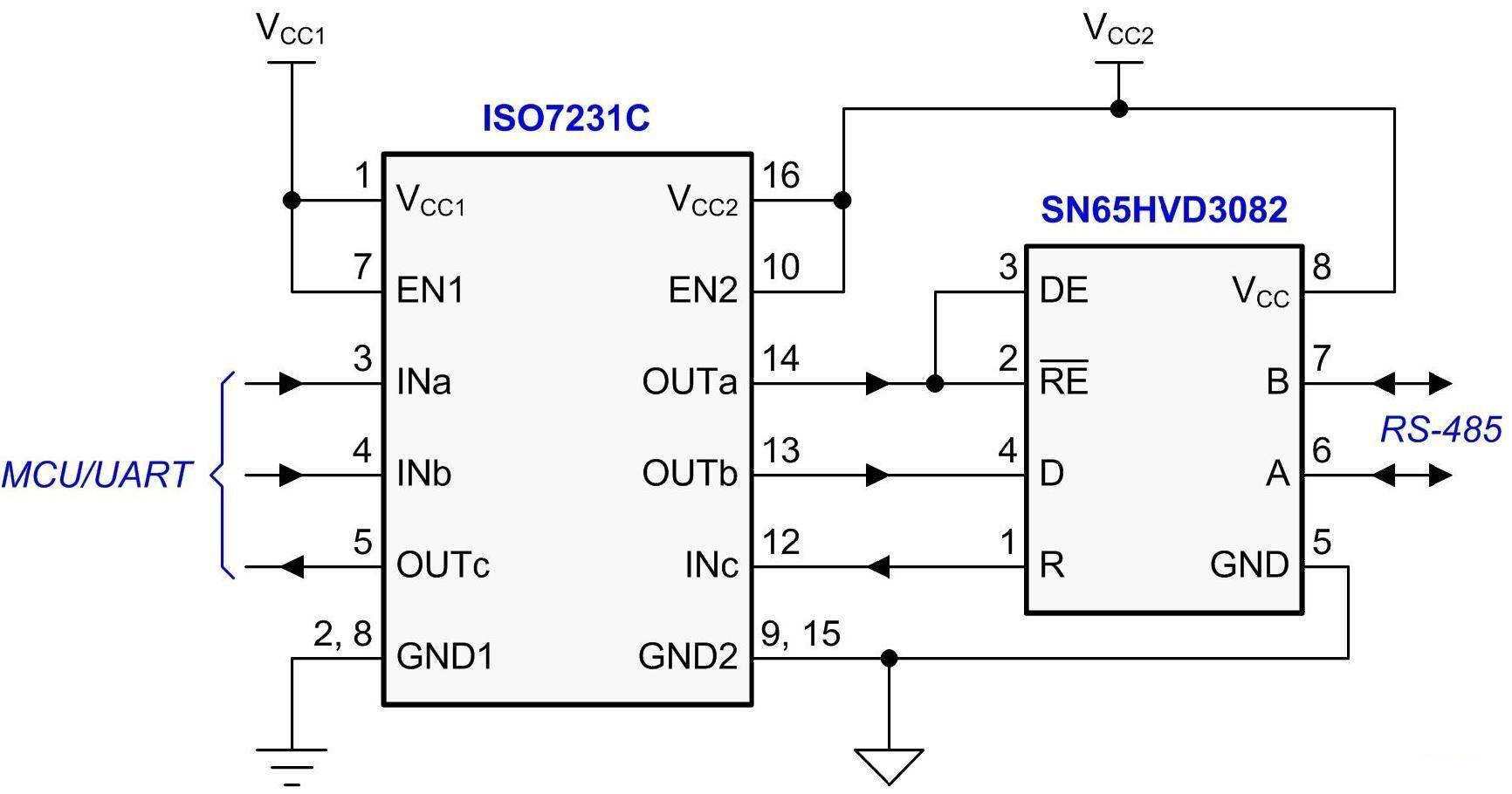
Supported by EEWorld Datasheet

Forum More
Update:2025-06-03 20:26:11

EEWorld
subscription
account

EEWorld
service
account

Automotive
development
community

Robot
development
community

About Us Customer Service Contact Information Datasheet Sitemap LatestNews


Room 1530, 15th Floor, Building B, No.18 Zhongguancun Street, Haidian District, Beijing, Postal Code: 100190 China Telephone: 008610 8235 0740

Copyright © 2005-2024 EEWORLD.com.cn, Inc. All rights reserved 京ICP证060456号 京ICP备10001474号-1 电信业务审批[2006]字第258号函 京公网安备 11010802033920号