Detailed introduction: https://blog.csdn.net/Ajisa_i/article/details/124731439?csdn_share_tail=%7B%22type%22%3A%22blog%22%2C%22rType%22%3A%22article%22%2C% 22rId%22%3A%22124731439%22%2C%22source%22%3A%22Ajisa_i%22%7D&ctrtid=EKJuC
Verification scheme is feasible. Type-c does not affect the use of the serial bus if it is not connected to the power supply. When the type-c is connected to the power supply, it can lead to 5v and 3.3v interfaces to supply power to the module. The board is simple, as long as you know the principle, you can use it in your own projects.
principle:
1. Hardware layer transformation
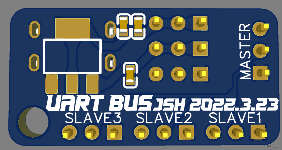
When the UART interface of the microcontroller we use is insufficient, we can use UART to implement a bus-type one-master-multi-slave communication structure, as shown in the figure.
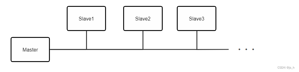
Figure 1 UART bus type communication structure
If you connect the slave's TX directly to the master's RX, then the TX pins between the slaves are connected together, as shown in Figure 2. When Slave1 tries to send information to the Master, since the UART starts with a low level, the TX pin of Slave1 is low level, while the TX pin of Slave2 is high level. At this time, the current flows from the TX pin of Slave2 to the TX pin of Slave1, and the current sink of the TX pin of Slave1 increases. Due to the internal resistance of the device, the increase in current causes the node p voltage to increase, and finally we see that the TX pin level of Slave1 increases.
Because the pin level rises, the RX end of the Master cannot receive the low level from the TX end of Slave1, and the serial communication cannot start.
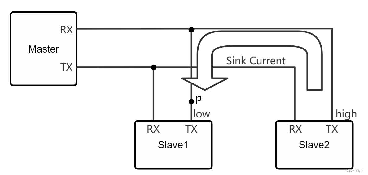
Figure 2 Sinking current causes the pin level to rise
One of the solutions is to set the slave's communication pin to an open-drain output. In open-drain output mode, the pin outputs neither high level nor low level under high-level logic, but is in a high-impedance state and requires an external pull-up resistor to output high level. Due to the existence of the pull-up resistor, the sink current is very small, thus avoiding the problem of rising pin level. However, we often cannot perform secondary development on the slave, that is, we cannot change the output mode of its communication pins.
Figure 3 shows another solution where the slave's TX pin is connected to the cathode of a diode and the diode anode is connected to the master's RX pin. Due to the unidirectional conductivity of the diode, the sink current will be limited to a very small range, which is equivalent to an open circuit, thereby avoiding the problem of the pin's low level rising. Since the RX pin of the host is in a pull-up input state, the high-level sampling will not be affected when the diode is turned off.
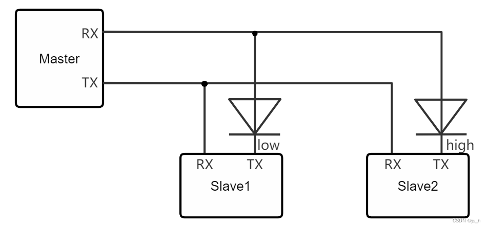
Figure 3 Using diodes to limit sink current
In fact, according to the principle, N+1 slaves only need N diodes. This is left to you to verify.

All reference designs on this site are sourced from major semiconductor manufacturers or collected online for learning and research. The copyright belongs to the semiconductor manufacturer or the original author. If you believe that the reference design of this site infringes upon your relevant rights and interests, please send us a rights notice. As a neutral platform service provider, we will take measures to delete the relevant content in accordance with relevant laws after receiving the relevant notice from the rights holder. Please send relevant notifications to email: bbs_service@eeworld.com.cn.
It is your responsibility to test the circuit yourself and determine its suitability for you. EEWorld will not be liable for direct, indirect, special, incidental, consequential or punitive damages arising from any cause or anything connected to any reference design used.
Supported by EEWorld Datasheet
EEWorld
subscription
account

EEWorld
service
account

Automotive
development
community

Robot
development
community

About Us Customer Service Contact Information Datasheet Sitemap LatestNews


Room 1530, 15th Floor, Building B,
No.18 Zhongguancun Street,
Haidian District,
Beijing, Postal Code: 100190
China
Telephone: 008610 8235 0740
 京公网安备 11010802033920号

 XC6105E433


