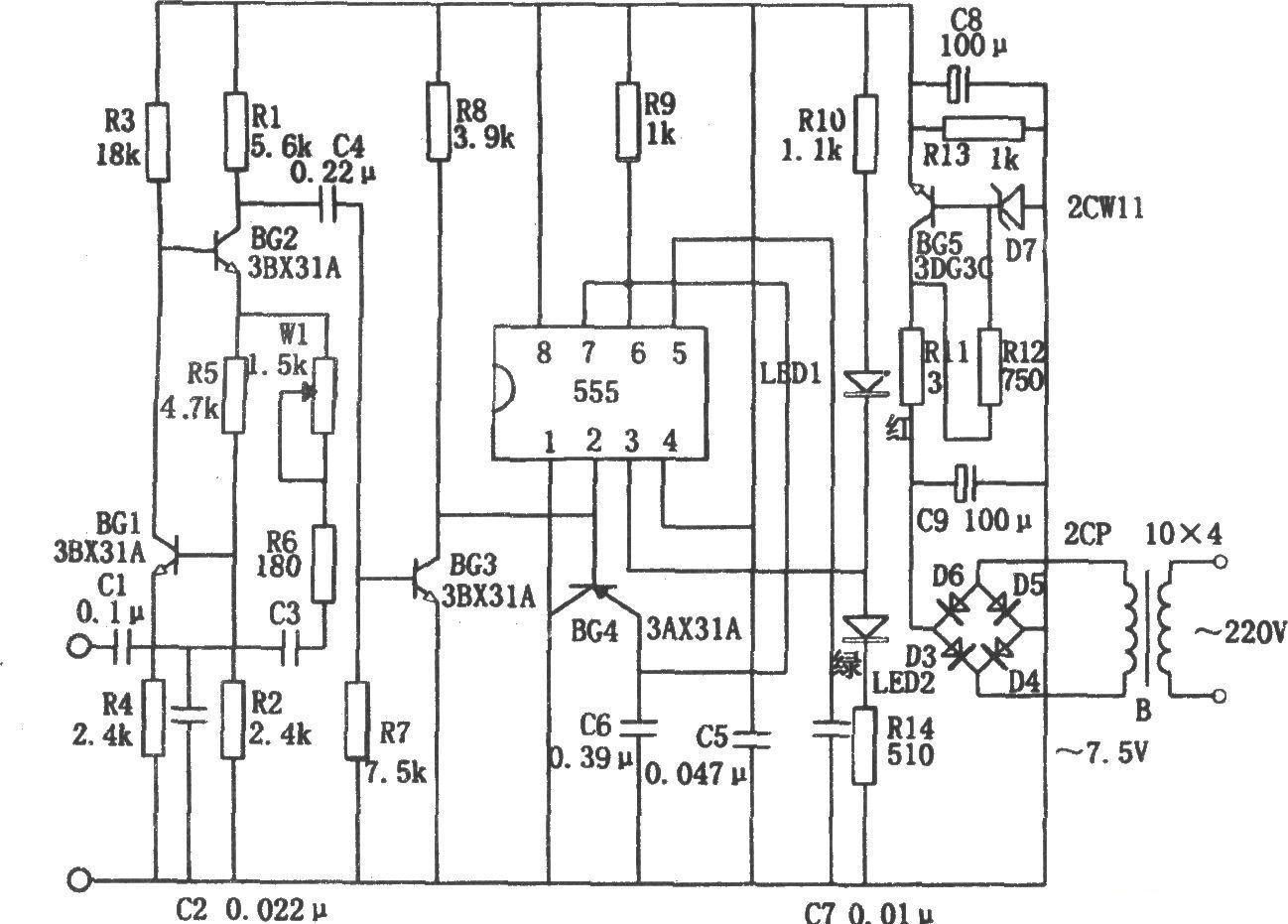
In the schematic diagram, the DP2 and DN2 network logos of the typec port are reversed. The positions are correct but the leads are reversed. I don’t know if this explanation is clear. The phenomenon is that the typec port is recognized when inserted from the front and not recognized when inserted from the back. This has been modified. Thanks to hkchenhao for pointing out the problem.
The design process and demonstration video are at Station B https://www.bilibili.com/video/BV1BS4y1N7Be?share_source=copy_web
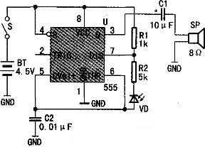
The MCU uses stm32f103c8t6, aluminum profile casing, and has 2 buttons for operation. The buttons are reused to realize the "up" and "down" button functions, as well as ISP download mode switching and power on and off functions. OLED displays temperature and voltage, op amp amplifies, MCU internal ADC samples soldering iron thermocouple voltage and current during heating. The code is generated using the Stm32CubeMX template. Functions currently implemented
1. Button to power on and off
1. Heat up the soldering iron
5. Indicator light, OLED screen
2. Adjust the temperature
3. Leave to sleep
4. ISP upgrade procedure

All reference designs on this site are sourced from major semiconductor manufacturers or collected online for learning and research. The copyright belongs to the semiconductor manufacturer or the original author. If you believe that the reference design of this site infringes upon your relevant rights and interests, please send us a rights notice. As a neutral platform service provider, we will take measures to delete the relevant content in accordance with relevant laws after receiving the relevant notice from the rights holder. Please send relevant notifications to email: bbs_service@eeworld.com.cn.
It is your responsibility to test the circuit yourself and determine its suitability for you. EEWorld will not be liable for direct, indirect, special, incidental, consequential or punitive damages arising from any cause or anything connected to any reference design used.
Supported by EEWorld Datasheet
EEWorld
subscription
account

EEWorld
service
account

Automotive
development
community

Robot
development
community

About Us Customer Service Contact Information Datasheet Sitemap LatestNews


Room 1530, 15th Floor, Building B,
No.18 Zhongguancun Street,
Haidian District,
Beijing, Postal Code: 100190
China
Telephone: 008610 8235 0740
 京公网安备 11010802033920号


 P4SMAJ40A-LFR