1. Refer to Essence’s ESP32-S development board schematic diagram for production, see the attached ESP32-S manual.

2. The CH340G (external crystal oscillator) used in this schematic diagram is compatible with CH340C (built-in crystal oscillator). The physical verification uses CH340C.
You can also modify and use other chips in the CH340 series. According to the video introduction, there should be DTR and RTS pins for automatic downloading, as shown below:

3. 5V to 3.3V using LDO AMS1117 output should be connected to a tantalum capacitor (the reason is detailed See video). Tantalum capacitors are polarized capacitors. Like electrolytic capacitors, they will explode if the polarity is reversed.

However, the 3D packaging of Lichuang EDA Professional Edition seems to be reversed. I changed one but couldn't find the right one, so I gave up and tried to get the right one.
Save it as a personal library and adjust 3D to match the polarity correctly:

4. Welding suggestions:
(1) First solder the USB type C socket. Since it uses 16 pins, it is a little difficult to solder. After soldering, confirm that there is no solder connection. You can use a multimeter to test the phase. Whether adjacent pins are short-circuited. The four fixed legs of the seat must be welded firmly to prevent them from being knocked over when connecting the data cable, causing the solder pad to tear and make you want to cry without tears. After confirming that the Type C socket has no connection, plug in the USB to power on, and test 5V with a multimeter before proceeding to the next step.


(2) Solder AMS1117 and use a multimeter to confirm that the 3.3V output is correct.
(3) Solder other components.
(4) Confirm that there is no soldering or tin ball residue, and clean it with washing water.
5. Verification:
For the ESP32-S development board, use Arduino to burn the Zhuque soldering station program for testing. The program can be successfully uploaded after multiple burning tests.


nodemcu-esp32_v1.3.pdf
61862
8838 Front and rear panels_GX12-F-5 through-wall aviation plug
Introduction: 8838 front and rear panels + GX12-F-5-core through-wall aviation plug
8838 front and rear panels + GX12-F-5-pin wall aviation plug.
The 5-pin wall aviation plug is not compatible with the 6-pin one! The 5-pin wall plug is not compatible with the 6-pin one! The 5-pin wall plug is not compatible with the 6-pin one!
1.T12 soldering station front panel, adapted to 8838 shell. For the following projects: Suzaku T12 soldering station
2. Only suitable for this 8838 shell: https://item.taobao.com/item.htm?spm=a1z09.2.0.0.3d712e8dYNNnYH&id=604087009395&_u=j6p063q484b
3. Used GX12- F-5-core through-wall aviation socket (easy to disassemble): https://item.taobao.com/item.htm?spm=a1z09.2.0.0.1c6a2e8dIILgHr&id=627942539887&_u=j6p063qcd45
4. Special statement: produced by each manufacturer The shell size is different, and others may not match. Please determine whether it is suitable, or please modify it before use. The links listed here have nothing to do with me and are for reference only.
5.
I forgot to select a color for the photo, so it was set to the default color green. White is recommended.


6. Reference materials:
The PCB copper foil windows and solder mask windows used in this project are used to transmit LED light, which has a hazy aesthetic and does not require PCB drilling. This idea comes from the power amplifier project of the boss HACK, and I would like to thank him.
BOM download
PCB_PCB_8838 front panel_GX12-F-5 through the wall_2022-09-22.pdf
PCB_PCB_8838 front panel_GX12-F-5 through the wall_2022-09-22.json
PCB_8838 front panel_GX12-F-5 wall penetration_2022-09-22.pcbdoc
Gerber_PCB_8838 front panel_GX12-F-5 through the wall_2022-09-22.zip
PCB_PCB_8838 front and rear panels_GX12-F-5 through the wall_2022-09-22.pdf
PCB_PCB_8838 front and rear panels_GX12-F-5 through the wall_2022-09-22.json
PCB_8838 front and rear panels_GX12-F-5 through the wall_2022-09-22.pcbdoc
Gerber_PCB_8838 front and rear panels_GX12-F-5 through the wall_2022-09-22.zip
61863
T12, handle integrated control panel, 616 version optimization, reed switch sleep
Introduction: All-in-one T12 soldering iron based on 616 circuit
重要更新v2.0 2022/3/19
一、来源:本电路基于网传(数码之家等)的616电路修改所得。至于616电路的起源,本人未完全考证(实际上,为啥叫616,暂没找到准确资料),据网上资料起源于一位叫more的大神(资料)。本项目也基于网上各种资料。使用P-Mos和N-Mos均可以制作t12控制板,但N-Mos需要自举升压电路,P-Mos版本电路更为简洁。文末参考资料增加了一篇N-mos版本的链接,感兴趣的网友自行前往。十分感谢各前辈打下的基础。
二、优势:电路简单可靠,升温迅速,能有效恒定温度。模拟电路,不受价格飞涨的芯片制约。物料成本极低,随意折腾不肉痛。
二、适用手柄:
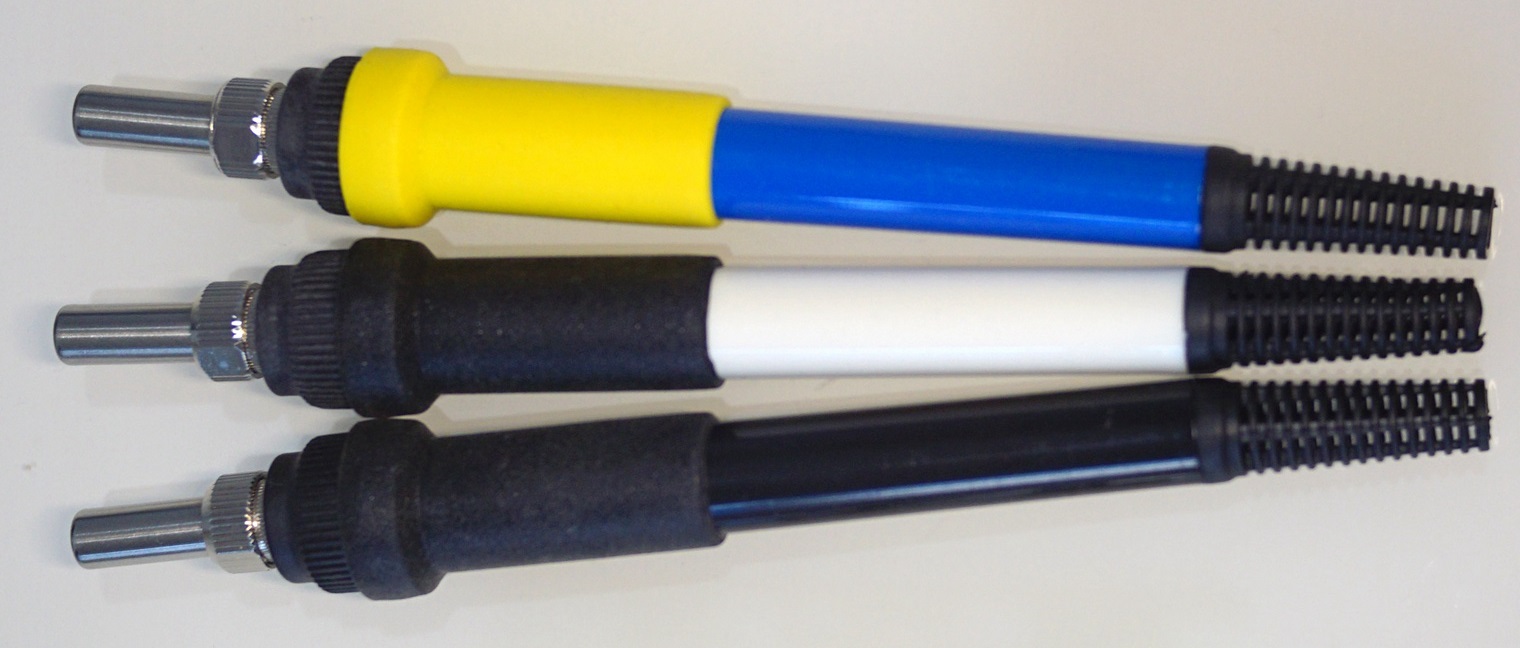
推荐使用白色手柄,可以透过led灯光。
三、改善要点:
(1)改善了LM358的2脚参考电压电路:由于R4远大于R8、R11和R12,以及R7远大于R8,因此R4和R7对LM358的2脚参考电压可以忽略,可以通过简单的电阻分压公式计算,并且计算时可以忽略R7。
(2)增加了干簧管休眠。休眠时LM358的2脚电压取决于R12的分压,因此,无论电位器调整为多少温度,休眠温度始终相同。烙铁架需要增加磁铁,即可使用休眠功能。
四、一些注意事项:
(1)控制板没能做的更短,其长度大于100mm;
(2)需要一个测温仪辅助。不同厂家生产的T12烙铁头,热电偶存在差异,不同的LM358也对温度产生不同程度的影响,R8、R11和R12的阻值分别决定最高温度、最低温度和休眠温度,图示阻值仅供参考,或者说,需要经过打板试样后,再适当调整。经测试,原616电路也存在该情况。
本电路也可以改成单独的控制板,将R8、R11和R12中一部分或者全部换成可调电阻,对最高温度、最低温度和休眠温度单独调节。
(3)我没有花精力去寻找更实用的电位器R7,实际使用中不便于调整温度。我将其调整为320℃,恒定温度使用。
(4)为减少pcb面积,pcb没有丝印,附件上传了手撸神器IBOM。
(5)元器件型号、封装直接参考立创EDA的BOM;但我没有在立创商城购买器件,供应商编号可能不准确。
五、修订历史:
v2.1 2022/3/22
pcb增加旋转45°版本,以满足10cm*10cm,不保证一定能成功通过审核打板。局部器件位置、布线优化。
v2.0 2022/3/19
数码之家网友@蕴殇打板了本工程,在其发布的帖子中引用了另一网友@飞菜鸟的帖子,他在该网友帖子第3楼的留言“当电位器接触不良时就出大事故了哦”,引起了我的注意。

我分析认为本工程也可能存在该潜在失效模式:当电位器接触不良等故障时,LM358第2脚悬空,电位不确定,可能引起比较器不能正常工作,导致温度失控。必须验证和改善。
查其他616电路图,以本开源平台另一616用的原理图为例,下图所示,由于R2和R3分压,当电位器VR1接触不良时,358第2脚实际上是最低温度的电压,没有上述风险。

风险验证:模拟电位器接触不良,直接移除电位器,这是电位器接触不良的极限状态,上电测试,果然,加热指示灯led1一直常亮,一大坨锡很快融化。

改善方法:找到原因,改善方法就有了,在358第2脚增加下拉电阻R20,这也是@飞菜鸟的改善方法。当电位器接触不良时,358第2脚电位被拉至地,停止加热。pcb的LM358旁边有一处空余地方,正好放置新增的电阻,pcb不用大改,简直不要太好。

改善措施验证1:保持电位器移除状态,使用10k直插电阻,连接358第2脚和GND,插入烙铁头上电测试,当使用12V供电时,红色加热指示灯低频率闪烁,约1到2秒闪烁1次,使用19.5V供电,指示灯闪烁频率更低,约5到6秒闪烁1次,实测温度均为70多度且保持恒定,实测358第2脚电压0.2mV。分析认为应是19.5V加热功率大,一个加热脉冲,温度就上去了,所以闪烁频率低;至于358第2脚为何电压不是零,限于对运放了解不足,暂无结论。

改善措施验证2:最后恢复电位器,测试电位器控温正常,休眠温度正常,且在各个电位器设置温度下,休眠温度仍基本无波动。至此认为改善有效。

v2.0版本的工程文件已经按上述改善方法增加电阻R20,pcb也同步完成更改。
已经使用v1.9版本打板的朋友,可按上述方法,用10k~100k的电阻,连接358第2脚和GND。当然,即使不飞电阻,也不见得一定出故障,但,即使是小概率事件,一旦识别,也应该预防其发生。
六、参考资料:
(1)白菜白光T12控制电路工作原理,两线发热芯如何实现加热与测温?
(2)T12烙铁的工作原理分析,看看T12就怎么样进行温控的
(3)白菜白光T12驱动电路解析
(4)给镂空搭棚T12加休眠功能
(5)使用NMOS场效应管的白光烙铁控制电路
(6)另有一些资料见附件
白菜白光电烙铁电路分析.rar
边框dxf_stp.rar
原理图_Gerber_iBom_v2.1.rar
BOM下载
PCB_PCB_45°_2022-09-22.pdf
PCB_PCB_45°_2022-09-22.json
PCB_45°_2022-09-22.pcbdoc
Gerber_PCB_45°.zip
PCB_PCB_2022-09-22.pdf
PCB_PCB_2022-09-22.json
PCB_2022-09-22.pcbdoc
Gerber_PCB.zip
Schematic_T12,手柄集成控制板,616版优化,干簧管休眠_2022-09-22.pdf
SCH_T12,手柄集成控制板,616版优化,干簧管休眠_2022-09-22.json
T12,手柄集成控制板,616版优化,干簧管休眠_2022-09-22.zip
Schematic_T12,手柄集成控制板,616版优化,干簧管休眠_2022-09-22.pdf
SCH_T12,手柄集成控制板,616版优化,干簧管休眠_2022-09-22.json
T12,手柄集成控制板,616版优化,干簧管休眠_2022-09-22.zip
61864
咩时钟
简介:小巧可爱 扩展性极强 价格低廉 的桌面时钟摆件 梦飞翔 esp8266 oled
This may be the smallest esp8266 OLED driver screen on the entire network. It
only requires at least one ams1117, one p6 usbc female socket, one esp12f and one ssd1306 screen (the capacitor and resistor can be omitted).
It is extremely easy to weld, and the gap is quite large. All you need is a hand
and it is still there. Supports swapping the positive and negative poles of the screen, welding the front and back sides, and is compatible with all i2c screen modules plug-in
source code https://github.com/zanjie1999/meClock-esp8266-oled
If it cannot be opened in mainland China, the mirror https://hub.fastgit.org /zanjie1999/meClock-esp8266-oled
BOM download
PCB_PCB_Mengfeixiang esp8266 oled_2022-09-22.pdf
PCB_PCB_梦飞飞 esp8266 oled_2022-09-22.json
PCB_Mengfeixiang esp8266 oled_2022-09-22.pcbdoc
Gerber_PCB_Mengfeixiang esp8266 oled_2022-09-22.zip
Schematic_咩clock_2022-09-22.pdf
SCH_咩clock_2022-09-22.json
Sheet_1_2022-09-22.schdoc
61865
USB extension adapter
Introduction: usbc to usbc to microusb to usba
Let's turn the redundant PD cables and data cables into new USB extension cables.
It can extend the USBC cable
, convert microUSB to USBC
, and even convert it into the most common USB.
Not only can it be charged, but it can also be used as an OTG.
BOM download
PCB_PCB_USB extension adapter_2022-09-22.pdf
PCB_PCB_USB extension adapter_2022-09-22.json
PCB_USB extension adapter_2022-09-22.pcbdoc
Gerber_PCB_USB extension adapter_2022-09-22.zip
Schematic_USB extension adapter_2022-09-22.pdf
SCH_USB extension adapter_2022-09-22.json
Sheet_1_2022-09-22.schdoc
61866
usb table interface conversion board (pd usb3.0)
Introduction: usb a to usb a 3.0 interface usb a to usb c for testing private fast charging protocol and PD protocol
Many cheap USB meters only have USB A port.
Use this adapter to connect USB meters with only USB A to USB C interface or USB3.0 interface for testing private fast charging protocol and PD protocol.
BOM download
PCB_usb table to usb3_2022-09-22.pdf
PCB_usb table to usb3_2022-09-22.json
usb table to usb3_2022-09-22.pcbdoc
Gerber_usb table to usb3_2022-09-22.zip
PCB_usb table to pd_2022-09-22.pdf
PCB_usb table to pd_2022-09-22.json
usb table to pd_2022-09-22.pcbdoc
Gerber_usb table to pd_2022-09-22.zip
PCB_usb table to pd-usb3_2022-09-22.pdf
PCB_usb table to pd-usb3_2022-09-22.json
Schematic_usb table interface conversion board (pd usb3.0)_2022-09-22.pdf
SCH_usb table interface conversion board (pd usb3.0)_2022-09-22.json
usb table interface conversion board (pd usb3.0)_2022-09-22.zip
usb table to pd-usb3_2022-09-23.pcbdoc
Gerber_usb table to pd-usb3.zip
61867
MA5671A/G-010S-A SFP debug version
Introduction: MA5671A/G-010S-A SFP debug version
MA5671A/G-010S-A SFP debugging version recommends using ch341a, etc.


BOM download
PCB_NOKIA3 copy_2022-09-22.pdf
PCB_NOKIA3 copy_2022-09-22.json
NOKIA3 copy_2022-09-22.pcbdoc
Gerber_NOKIA3 copy_2022-09-22.zip
61868
MA5671A/G-010S-A SFP flashing board
Introduction: MA5671A/G-010S-A SFP flashing board, can be used for soldering pins
MA5671A/G-010S-A SFP flashing board, can be used for soldering pins

BOM download
PCB_PCB_NOKIA 5671A 3_2022-09-22.pdf
PCB_PCB_NOKIA 5671A 3_2022-09-22.json
PCB_NOKIA 5671A 3_2022-09-22.pcbdoc
Gerber_PCB_NOKIA 5671A 3_2022-09-22.zip
61869
Electromagnetic gun board (separated)
Introduction: Can die
The hierarchical electromagnetic acceleration
photoelectric switch was bought on Taobao
and is still being tested .
The coil is hand-wound.
BOM download
PCB_Entire (impossible)_2022-09-22.pdf
PCB_Entire (impossible)_2022-09-22.json
The whole (impossible)_2022-09-22.pcbdoc
Gerber_entire(impossible).zip
PCB_PCB_separated copy copy_2022-09-22.pdf
PCB_PCB_separated copy copy_2022-09-22.json
PCB_separated copy copy_2022-09-22.pcbdoc
Gerber_PCB_separated copy copy_2022-09-22.zip
PCB_PCB_separated copy_2022-09-22.pdf
PCB_PCB_separated copy_2022-09-22.json
Schematic_Electromagnetic gun board (separated)_2022-09-22.pdf
SCH_Electromagnetic gun board (separated)_2022-09-22.json
Electromagnetic gun board (separated)_2022-09-22.zip
61870
electronic


 京公网安备 11010802033920号

 HSP43481/883


