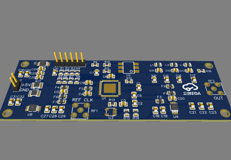
This project is used for the solution verification of AD9912ABCPZ-REEL7 ([Product No.: C408403](https://item.szlcsc.com/397673.html) [Lichuang Mall](https://www.szlcsc.com/) version design.
This project is [EDA Open Source Hardware Platform](https://oshwhub.com/) [Solution for Solution Verification Module](https://oshwhub.com/rewards/f4bbab6365034e80aadb8f8ebf77c846) sample project
. The digital synthesizer (DDS) is characterized by an integrated 14-bit digital-to-analog converter (DAC), including an integrated comparator, and its output signal is a square wave or sine wave with a 48-bit frequency control word (FTW). , can achieve frequency resolution of 4uHz, and can obtain absolute frequency accuracy by adjusting the DAC system clock.
AD9912 also provides an integrated system clock phase-locked loop (PLL) operating system clock input as low as 25MHz.
AD9912 features:
1. 1G internal clock. (Direct output up to 400MHz);
2. Integrated 1GSPS 14bit DAC;
3. 48bit frequency control word, 4uHz frequency resolution;
4. Differential HSTL comparator;
5. Flexible system clock input, can use crystal oscillator or external Reference clock;
6. On-chip low-noise PLL reference clock multiplication;
7. 2 SpurKiller channels;
8. Low-jitter clock multiplier up to 750MHz;
9. Single-ended CMOS comparator, frequency less than 150MHz;
10. CMOS output Programmable output divider;
11. Serial control;
The external clock reference is connected to the SYSCLK pin of the AD9912 to generate the internal high-frequency system clock.
The SYSCLK input can operate in the following three modes:
1. Without system clock phase locking. ring;
2. Use the system clock phase-locked loop and the externally generated input signal;
3. Use the system clock phase-locked loop and the crystal oscillator;
when the functional circuit of the system clock phase-locked loop frequency multiplier is disabled, the AD9912 must have a high frequency Signal source driver (250MHz~1GHz), the signal is input from the system clock input pin, and becomes the internal DAC sampling clock through the internal buffer.
When the system clock phase-locked loop frequency multiplier is enabled, the input frequency of the system clock input pin. The maximum input frequency allowed by the system clock phase-locked loop phase detector cannot be exceeded.
The AD9912 has two output drivers. The primary output driver supports 1.8V HSTL differential output levels and the second driver supports 1.8V or 3.3V CMOS levels. .

