This is a four-switch Buck-Boost digital power supply based on the STM32G474, supporting Type-C interface PD decoy input and DC 5.5 interface input, with a maximum input/output of 48V 10A. This is my graduation project, now open-sourced, including schematics, PCB layout, source code, and a 3D model of the casing.
It's not great, so please be kind and welcome friendly discussion.
Demo video: https://www.bilibili.com/video/BV1Ui421y7ip/
Open-source intelligent electronic load based on CH32V307, embedded system competition project open-source: https://blog.zeruns.tech/archives/785.html
Electronics/Microcontroller Technology Exchange QQ Group: 820537762
Download links are at the end of the article.
The circuit was designed using JLCPCB EDA software, which is really useful.
Introduction
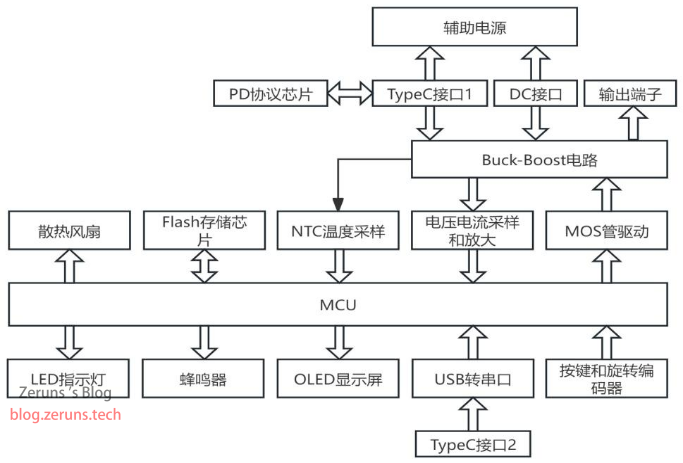
This paper designs a synchronous rectified Buck-Boost digital power supply based on STM32. The power supply circuit consists of a MOSFET driver circuit, a 4-switch Buck-Boost circuit, a signal conditioning circuit, a PD fast charging protocol circuit, an auxiliary power supply circuit, and a microcontroller control circuit.
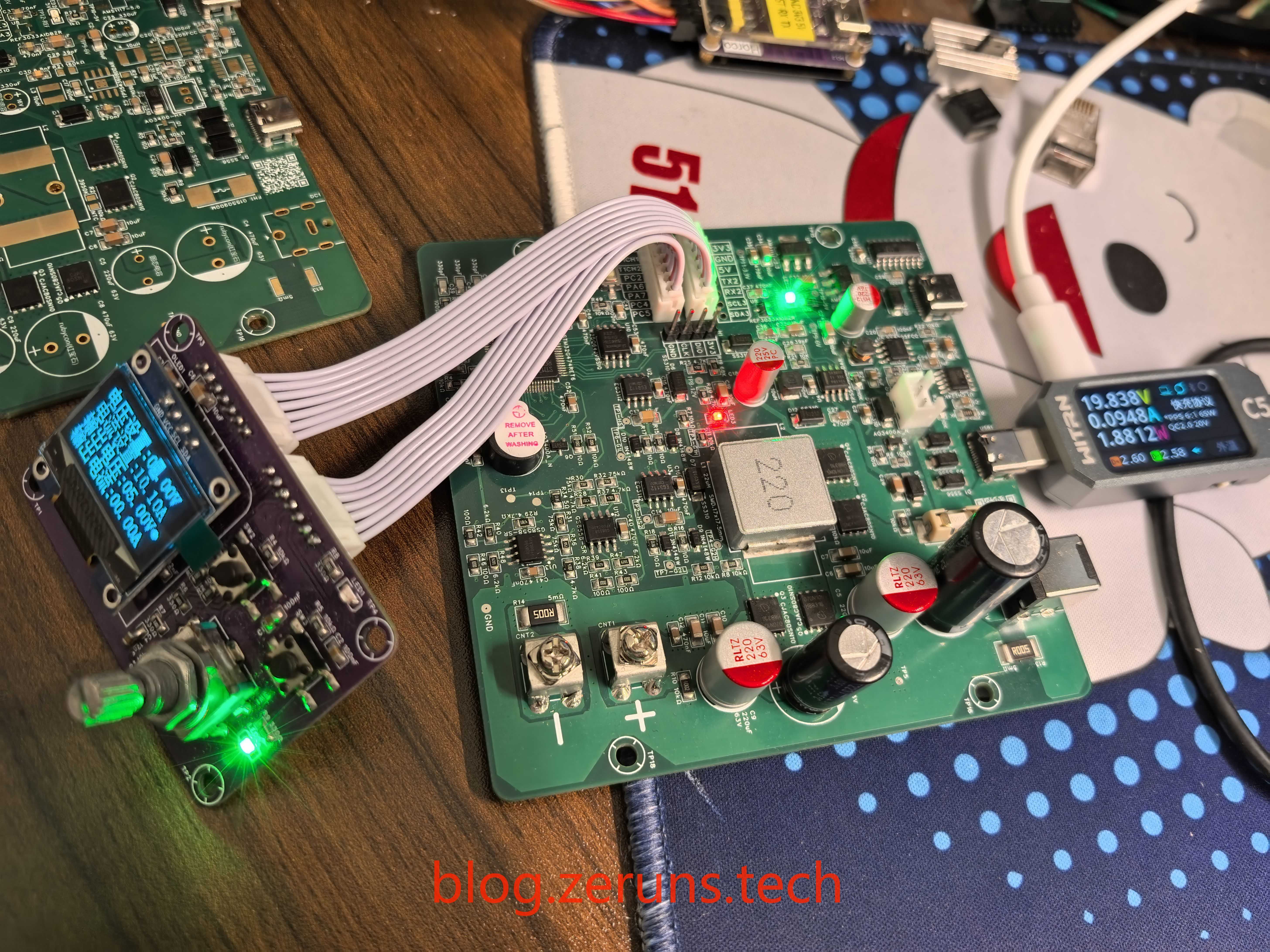
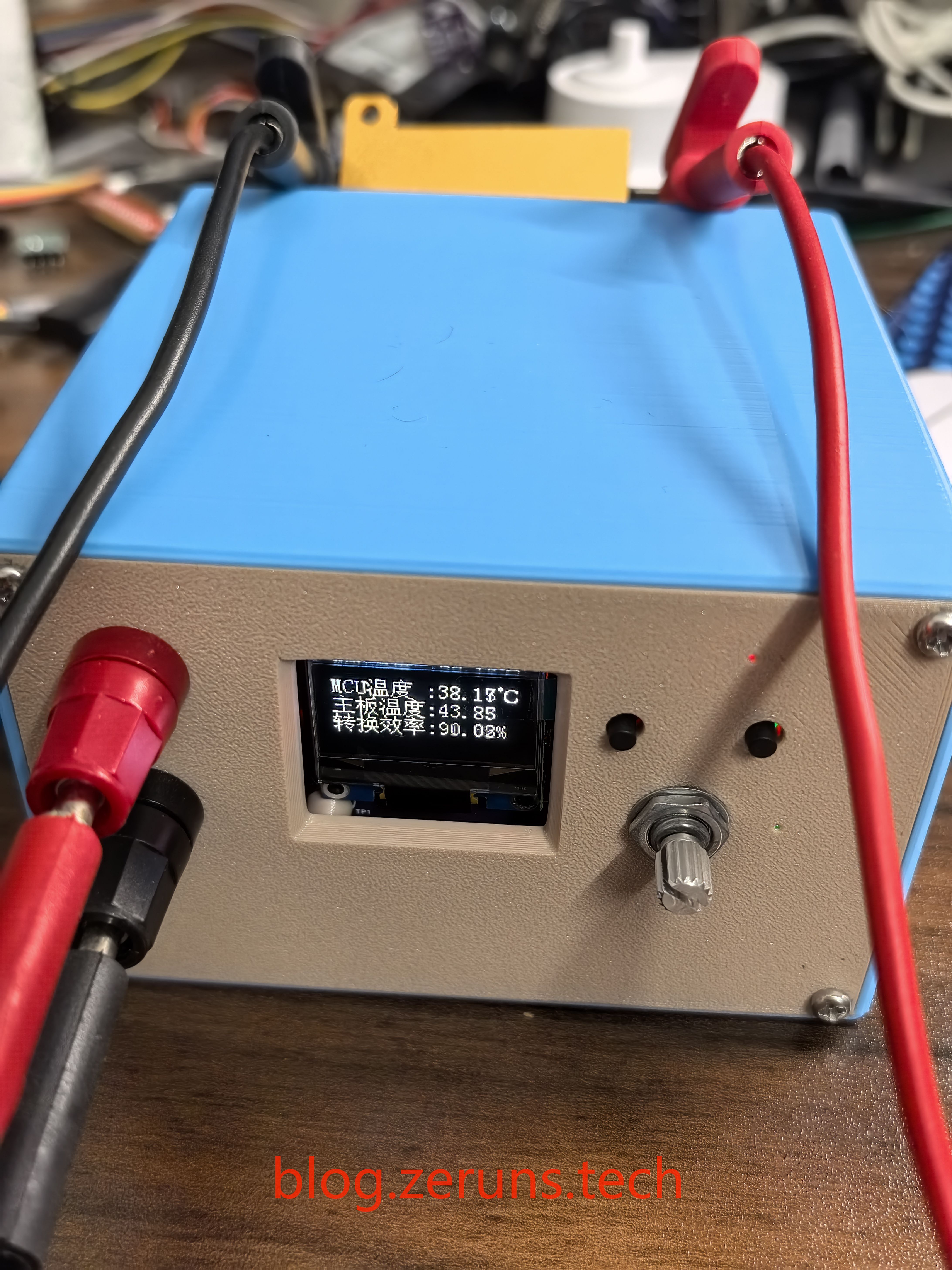
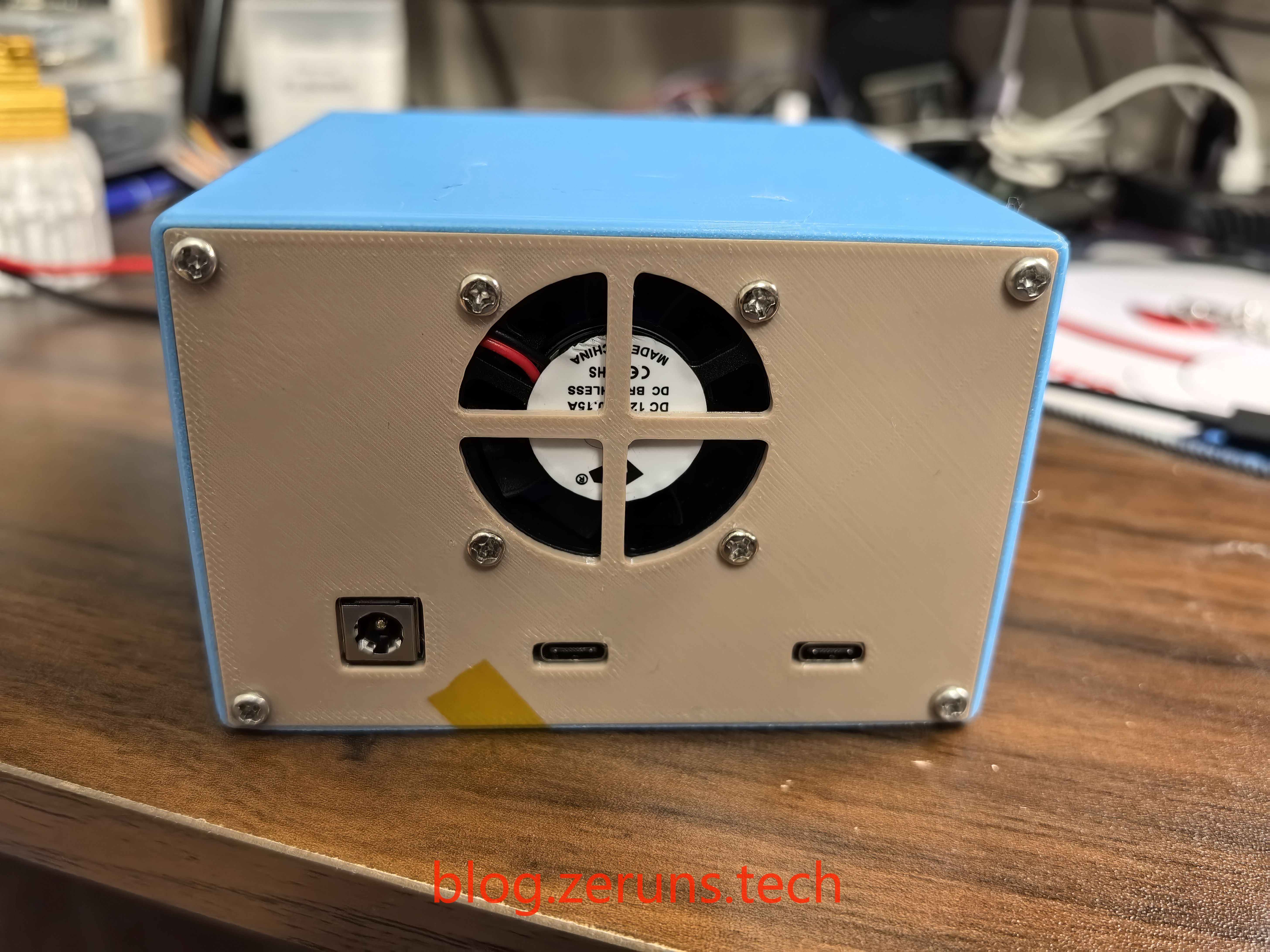
The power supply can be powered via a DC interface or a Type-C interface. The Type-C interface supports communication with the charger via the PD fast charging protocol, automatically requesting and obtaining a maximum operating voltage of 20V. The power supply uses an STM32G474 microcontroller to monitor the input and output voltage and current in real time, and uses a PID control algorithm to adjust the output PWM duty cycle, implement overvoltage and overcurrent protection, and sample the motherboard temperature for overtemperature protection. Furthermore, the power supply parameters can be viewed in real time on an OLED screen, and the output voltage and current can be set via a rotary encoder and buttons. It can also communicate with a host computer via another Type-C interface, allowing real-time viewing of various power supply parameters and waveforms through the host computer software.
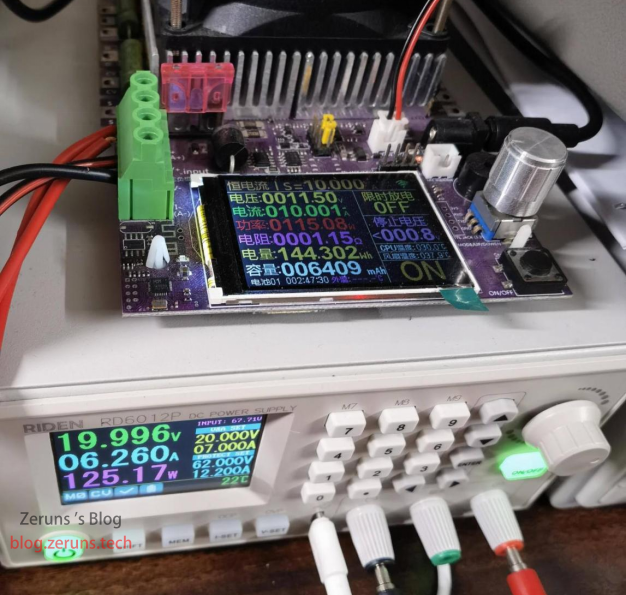
Design Performance Parameters The power
supply design performance parameters are shown in the table below:
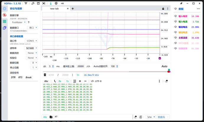
| Item |
Parameter | | ---|---|---| ---| | Input Voltage Range | 12Vdc~48Vdc | | Input Current Range | 0~10A | | Maximum Output Power | 450W | | Output Voltage Range | 0.5Vdc ~48Vdc | | Output Current Range | 0~10A | | Output Voltage Ripple | Peak-to-Peak Value ≤200mV | | Switching Frequency | 181.333kHz | Physical Diagram Using VOFA+ as the host computer software, various power supply parameters (input voltage and current, output voltage and current, motherboard temperature, MCU temperature, power conversion efficiency, etc.) and waveform changes can be viewed in real time. See the figure below. System Framework Diagram | Hardware Circuit Design | Component Selection Calculation | Inductor Calculation In synchronous BUCK-BOOST power supplies, inductor calculation needs to consider the operating conditions in BUCK and BOOST modes to ensure that the circuit's operating requirements are met in both modes. Typically, the inductor selection is based on the mode with the higher inductor requirement. When the power supply operates in buck mode, assuming a maximum input voltage of 48V and a minimum output voltage of 5V, calculate the minimum PWM duty cycle: $$ D{min} = frac{V{out_min}}{V_{in_max}} = frac{5V}{48V} = 10.417% $$ Define the inductor current fluctuation (25% of the maximum rated current ripple, assuming the maximum rated current is 10A): $$ Delta IL = 25% cdot I{out_nom} = 25% imes 10A = 2.5A $$ Calculate the minimum required buck inductor: $$ L{minBuck} = frac{V{out_min}}{Delta IL cdot f{switch}} = frac{5V}{2.5A imes 181333Hz} imes (1 - 10.417%) approx 9.88mu H $$ When the power supply operates in BOOST mode, the PWM duty cycle is calculated using the input rated voltage of 24V as the calculation point: $$ D{Bo} = 1 - frac{V{in_nom}}{V_{out_max}} = 1 - frac{24V}{48V} = 50% $$ In Boost mode, when 1A ($I_{minb}$) is taken, Boost enters continuous mode (CCM), and the inductance is calculated: $$ L{minBoost} = frac{V{out_max} cdot D{Bo}(1-D{Bo})^2}{2 cdot I{minb} cdot f{switch}} = frac{48V imes 50% imes (1 - 50%)^2}{2 imes 1A imes 181333Hz} = 16.544mu H $$ Based on the calculation results obtained from the formula, the minimum inductance value required to meet the predetermined ripple current requirement is determined. To ensure this condition is met, an inductor with a value slightly higher than the calculated value should be selected. Simultaneously, it must be ensured that the selected inductor's saturation current can handle the highest peak current in the circuit. Since efficiency factors are not considered in the calculations, the actual duty cycle and peak current may be lower than the theoretically calculated values. Therefore, a certain safety margin should be considered when selecting an inductor to accommodate various situations that may occur under actual operating conditions. Taking all the above factors into account, this design selects a 22μH inductor with a saturation current of 10A or higher in a 1770 surface mount package as the inductor for the BUCK-BOOST circuit. Capacitor Calculation To obtain a better output voltage ripple, the designed voltage ripple is taken as 50mV. $$ Delta V_{out} = 0.05V $$ The inductor selected above is 22μH, so this inductance value is also used in the calculation here: $$ L_{BB}=22mu H $$
Calculate the minimum capacitances $C{minBuck}$ and $C{minBoost}$ required for operation in BUCK and BOOST modes respectively:
$$
C{minBuck}=frac{V{out_min}cdot(1-frac{V{out_min}}{V{in_max}})}{8cdot L{BB}cdot Delta V{out}cdot {f_{switch}}^2}=15.48mu F
$$
$$
C{minBoost}=frac{I{out_nom}cdot(1-frac{Vin_min}{Vout_max})}{Delta Voutcdot fswitch}=413.6mu F
$$
The design needs to leave a certain margin and for lower output ripple, so a 220μF low-ESR solid capacitor and a 470μF ordinary electrolytic capacitor are selected, for a total of 690μF.
MOSFET Selection Calculation:
Within the rated input and output voltage range, the effective value of the input MOSFET current is calculated as:
$$
i_{mos_rms}=7.098A
$$
The rated current value $I_D$ of the MOSFET in the selection process should be more than twice the maximum current flowing through the MOSFET (to prevent excessive current from causing impact damage under fault or short circuit conditions).
$$
2×i_{mos_rms}=14.196A
$$
The rated withstand voltage $V_{DS}$ of the selected MOSFET must be greater than 1.5 times the maximum input voltage (to prevent spike breakdown)
$$
1.5×Vin_max=72V
$$
After referring to the previous calculations, for typical applications, a MOSFET with a rated current exceeding 15 amps (A) and a withstand voltage of 100 volts (V) can be selected. The selection of the lower MOSFET is the same as that of the upper MOSFET. Considering heat generation, in order to minimize energy loss during conduction and switching, a MOSFET with low on-resistance ($R_{DS(on)}$) and low output capacitance (Coss) should be preferred.
The MOSFET selected in this design is CJAC80SN10, which is manufactured by Jiangsu Changjing Technology Co., Ltd. and is a domestically produced MOSFET. It has a drain-source withstand voltage of 100V ($V_{DS}$) and a maximum drain-source current of 80A ($ID$). Its on-resistance ($R{DS(on)}$) is only 6.2mΩ, a low-resistance characteristic that helps reduce power loss in the on-state. Simultaneously, the device's output capacitance Coss has a typical value of 420pF, a low capacitance that helps reduce dynamic losses during switching. Therefore, the CJAC80SN10 meets the electrical characteristics required by the project while effectively reducing energy loss and improving the overall system efficiency.
Power Board Circuit Design:
Main Power Circuit
The following diagram shows the main power circuit of the synchronous BUCK-BOOST power supply. The left side is the input. The synchronous BUCK buck circuit consists of MOSFETs Q2 and Q4 and inductor L1, while the synchronous BOOST boost circuit consists of MOSFETs Q3 and Q5 and inductor L1. A 10kΩ resistor is connected between the gate and source of each MOSFET to ensure that the MOSFET gate is not floating and to prevent malfunction.

The main power circuit has a symmetrical structure, with one 470μF/63V aluminum electrolytic capacitor and one 220μF/63V solid aluminum electrolytic capacitor at both the input and output terminals. Additionally, there are two small surface-mount MLCC (multilayer ceramic capacitors) with parameters of 10μF/50V, used to filter high-frequency noise interference at the ports. R9 and R10 act as dummy loads at the input and output ports, quickly dissipating residual energy when the power is off. R13 and R14 are high-precision 5mΩ resistors used for current sampling, which are then connected to a differential amplifier circuit to amplify the input and output current signals. CNT1 and CNT2 are output terminals. L1 and L2 are a surface-mount 1770 package and a through-hole magnetic ring inductor package, respectively; only one needs to be soldered. Drawing both is for easy testing of the effects and performance of different inductors.
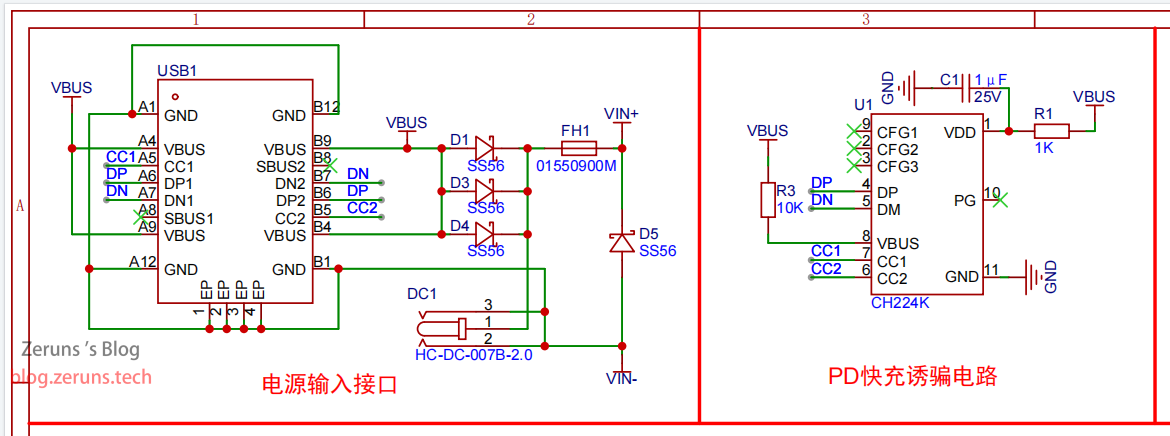
Power Input and Fast Charging Protocol Circuit
The following diagram shows the power input interface and the circuit diagram for PD fast charging protocol communication.
The power input uses two interfaces: a DC 5.5*2.5mm female connector and a Type-C female connector. The Type-C connector supports multiple fast charging protocols such as BC1.2 and PD3.0/2.0, using the CH224K fast charging protocol chip. It can communicate with fast chargers to enable the charger to output a maximum voltage of 20V, supporting a maximum power of 100W.
Diodes D1, D3, and D4 prevent the DC interface voltage from flowing back into the Type-C interface; the design does not allow both interfaces to be connected simultaneously. D5 is a diode for reverse connection protection. FH1 is the power input fuse holder, which accepts a 12A fuse.
In
the synchronous BUCK-BOOST power supply design, both the BUCK and BOOST circuits include high-side N-MOSFETs. Traditionally, these high-side N-MOSFETs are driven using transformer-isolated drives, but this method increases circuit complexity and board size.
This design uses two EG3112 MOSFET driver chips with built-in bootstrap circuitry to drive the MOSFETs in the BUCK and BOOST circuits. The EG3112 is a non-isolated complementary dual-channel driver chip; its 2A output drive current capability ensures rapid MOSFET turn-on; the chip also incorporates dead-time control to prevent shoot-through of the output drive signal, thereby improving system stability. The specific circuit is shown in the figure below.
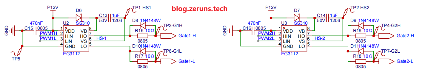
Taking the MOSFET drive of the BOOST boost circuit as an example, PWM2L and PWM2H are PWM signals output from the STM32G474 microcontroller and fed into the LIN and HIN pins of the EG3112 driver chip. LO is the lower MOSFET drive signal output with a 10Ω drive resistor, HO is the upper MOSFET drive signal output with a 10Ω drive resistor, D7 is the bootstrap diode for the upper MOSFET drive circuit, D9 and D11 diodes are used to quickly release the gate charge and accelerate the MOSFET turn-off speed, and C14 is the bootstrap capacitor.
The driving resistor is used during MOSFET switching because the driving signal may cause reflections and oscillations on PCB traces, distributed capacitance, inductance, and other components. Connecting a series resistor reduces these oscillations, improving system stability and reliability.
Auxiliary Power Supply:
The following diagram shows the schematic of the auxiliary power supply circuit on the power board.
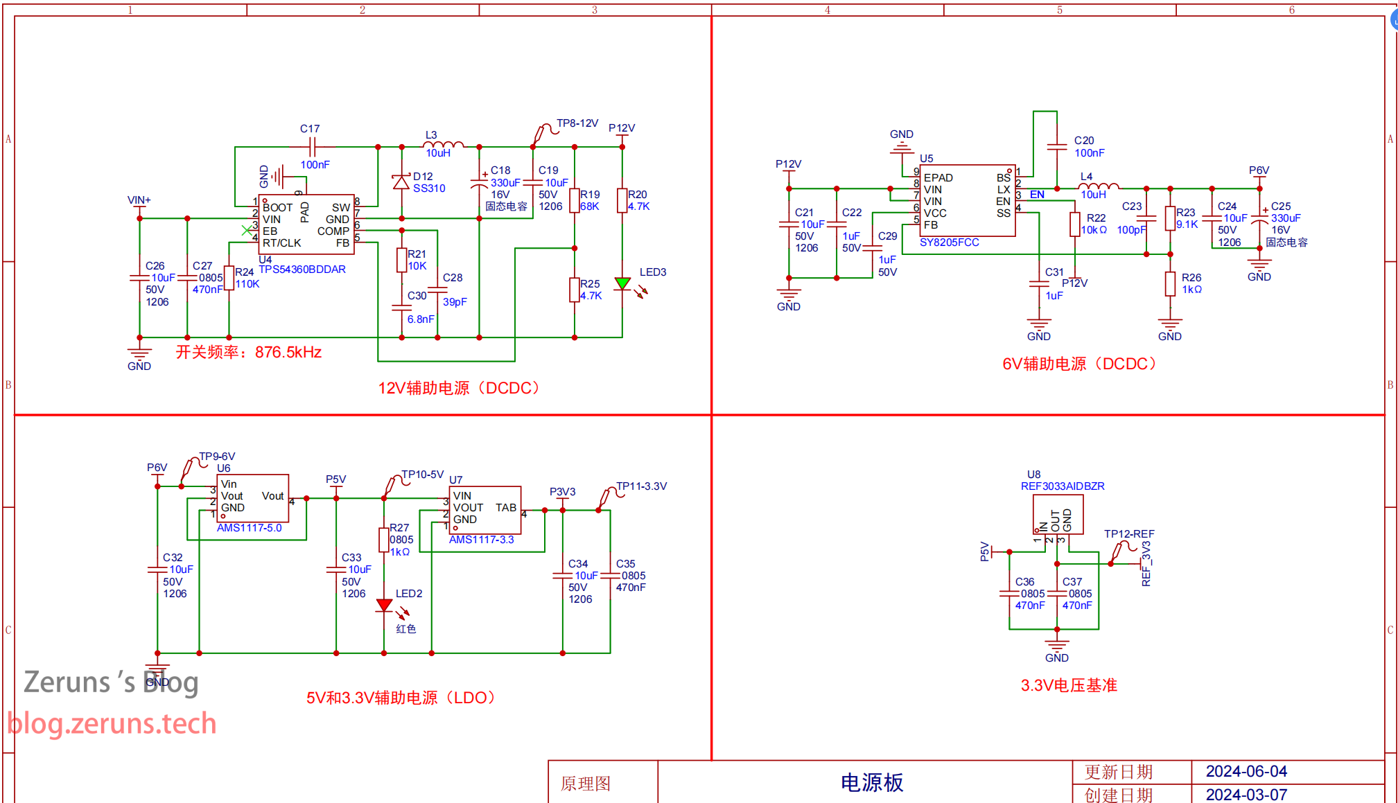
The auxiliary power supply circuit for the first-stage 12V output uses the TPS54360B BUCK-type power chip with integrated high-side MOSFETs. According to the chip's datasheet, a pull-down resistor connected to the RT pin can set the switching frequency; a 110kΩ resistor is selected here, corresponding to a switching frequency of 876.5kHz. For higher switching frequencies, a smaller inductor can be used to save space. Based on this frequency, the inductor value should be greater than 9.75μH; a 10μH inductor is selected here, and an SS310 freewheeling diode is chosen. C26 and C27 are input filter capacitors; the feedback voltage divider resistors R19 and R25 divide the voltage to provide a 0.8V reference voltage to the chip's FB pin, ensuring the output voltage is 12V. C18 and C19 are filter capacitors for the first-stage 12V output auxiliary power supply. The first-stage 12V output mainly supplies the input to the second-stage 6V buck circuit, as well as the MOSFET driver circuit and cooling fan.
The auxiliary power supply circuit for the second-stage 6V output uses the SY8205 synchronous rectification BUCK power chip with integrated MOSFETs. According to the chip datasheet, the chip's switching frequency is fixed at 500kHz, and the inductor in the auxiliary power supply BUCK circuit is selected as 10μH. C21 and C22 are input filter capacitors; feedback voltage divider resistors R23 and R26 divide the voltage to provide a 0.6V reference voltage to the chip's FB pin to ensure the output voltage is 6V. C24 and C25 are filter capacitors for the second-stage 6V output auxiliary power supply. Since directly using a linear regulator to step down from 12V to 5V would cause significant losses, a switching power supply is first used to step down the voltage to near 5V, and then a linear regulator is used to step it down to the target voltage. This ensures higher efficiency and lower output ripple.
The 6V output voltage from the second stage is stepped down to 5V by the AMS1117-5 linear regulator chip as the third-stage auxiliary power supply. The voltage reference chip REF3033 is used for signal conditioning, OLED display, USB communication, and other functional circuits.
The 5V DC power is stepped down to 3.3V by the AMS1117-3.3 linear regulator chip as the fourth-stage auxiliary power supply for the MCU, buzzer, Flash chip, and other circuits.
The REF3033 voltage reference chip outputs a 3.3V reference voltage for the MCU's VREF port, serving as the reference voltage for the MCU's built-in ADC and improving the ADC's sampling accuracy.
The signal conditioning circuit
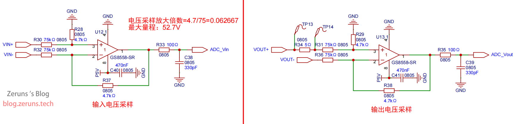
, as shown in the diagram, employs differential amplification technology for the input and output voltage sampling and signal conditioning circuits. The differential amplification topology effectively reduces the interference of high-frequency noise in the switching power supply on the signal conditioning circuit, improving signal stability and reliability. In this circuit, a low-bias operational amplifier, the GS8558-SR, is selected to improve conversion accuracy. The GS8558-SR op-amp has excellent DC accuracy and low bias current characteristics, which are crucial for improving the overall performance of the signal conditioning circuit.
Feedback resistors of the differential amplifier circuit:
$$
R_{38}=4.7kΩ
$$
$$
R_{36}=75kΩ
$$
Calculate the differential gain:
$$
KV=frac{R{38}}{R_{36}}=0.062667
$$
The maximum sampling voltage of the MCU's ADC is 3.3V output from the voltage reference chip. Therefore, the maximum value of the input and output voltage that can be sampled can be calculated as:
$$
V_{max}=frac{3.3V}{K_V}=52.66V
$$
To better suppress the interference of high-frequency noise in the switching power supply on the differential amplifier circuit, decoupling capacitors C40 and C41 are added to the power supply pins of the op-amp for filtering. MLCC (multilayer ceramic capacitors) are selected for the capacitors. MLCCs have lower ESR and ESL, and have better filtering effect in high-frequency noise. At the same time, resistor R35 and capacitor C39 are added to the output to form an RC low-pass filter circuit to filter out high-frequency noise.

As shown in the diagram above, the input and output current conditioning circuits use differential amplification. The output current sampling resistor is:
$$
R_{14}=5mΩ
$$
The feedback resistor of the differential amplifier circuit is:
$$
R_{48}=6.2kΩ
$$
$$
R_{46}=100Ω
$$
The differential amplification factor is calculated as:
$$
KI=frac{R{48}}{R_{46}}=62
$$
That is, 310mV is output for every 1A of current.
The maximum sampling voltage of the MCU's ADC is 3.3V, which is the output of the voltage reference chip. Therefore, the maximum value of the input and output current that can be sampled is calculated as:
$$
I_{max}=frac{3.3V}{KI imes R{14}}=10.65A
$$
MCU Control Circuit
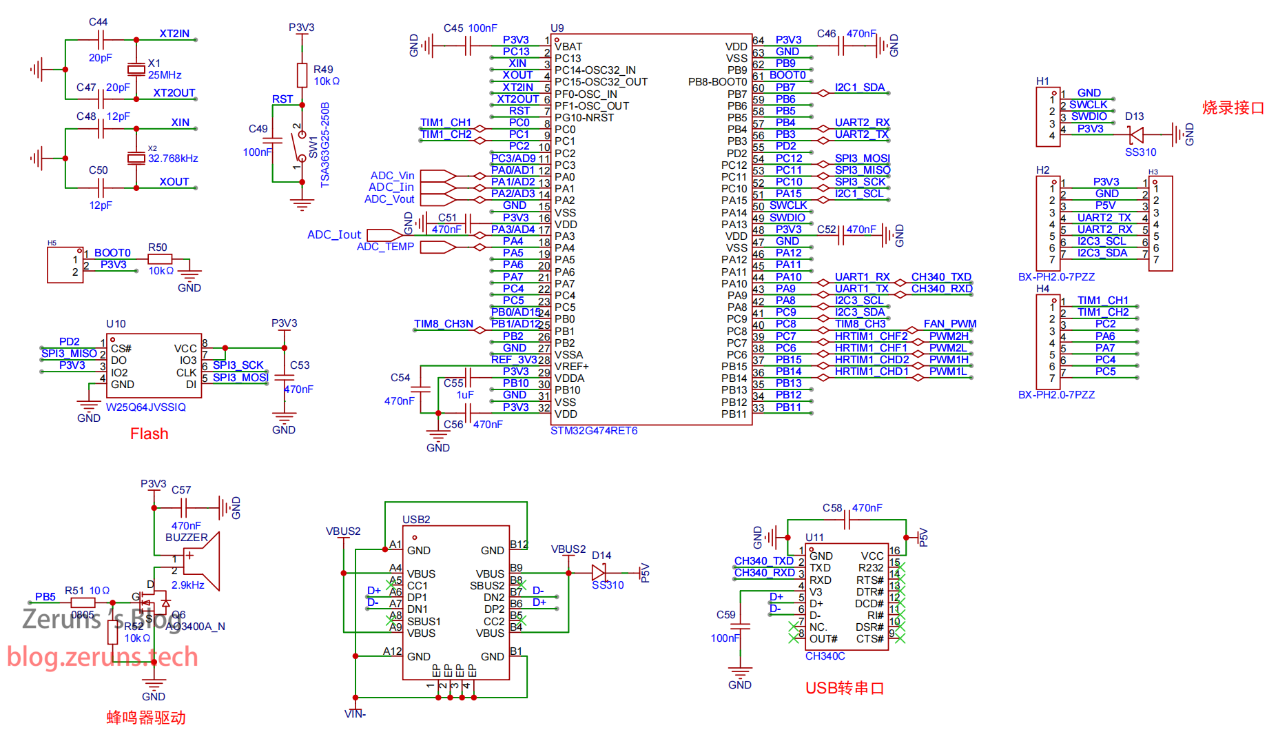
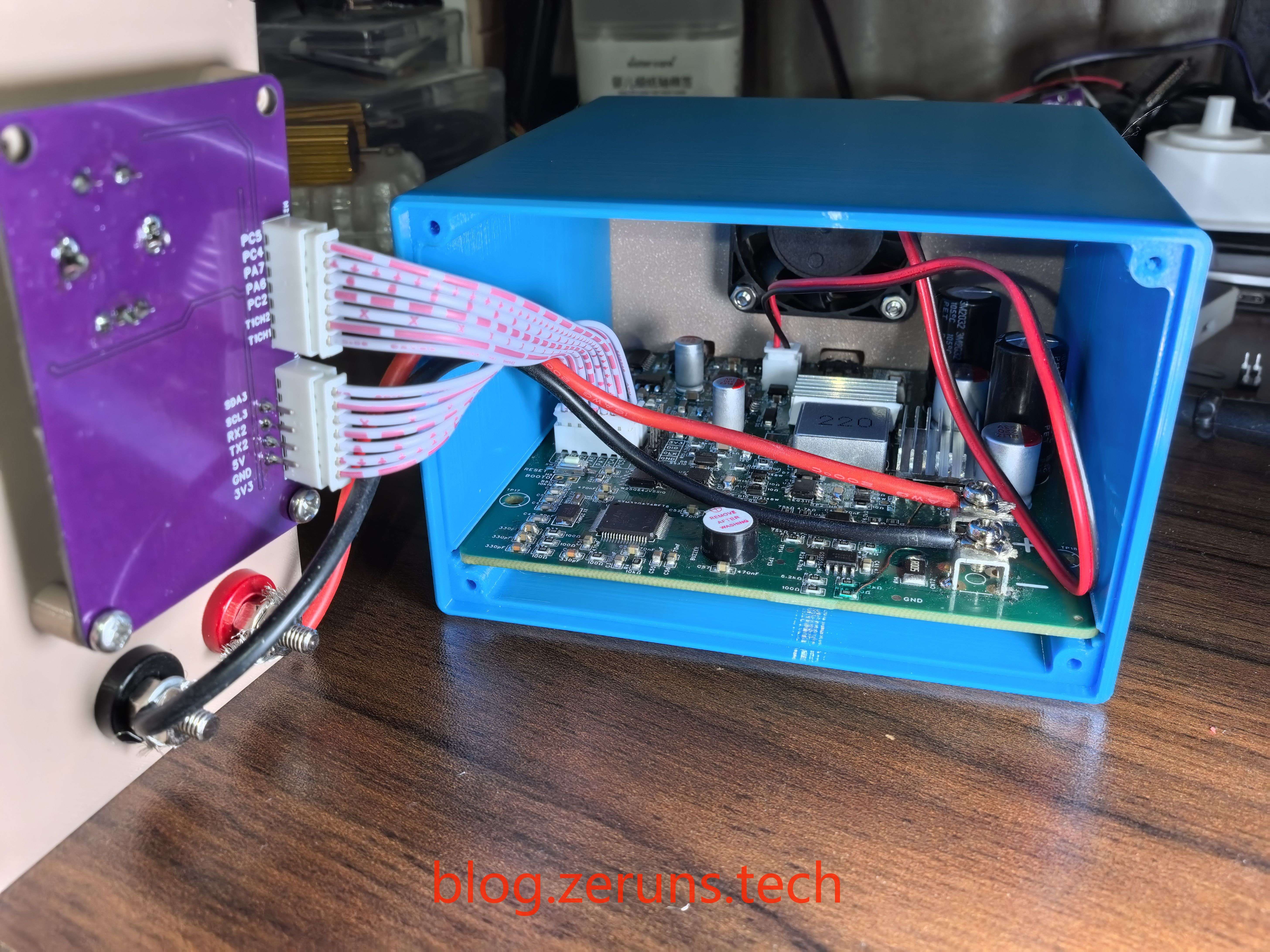
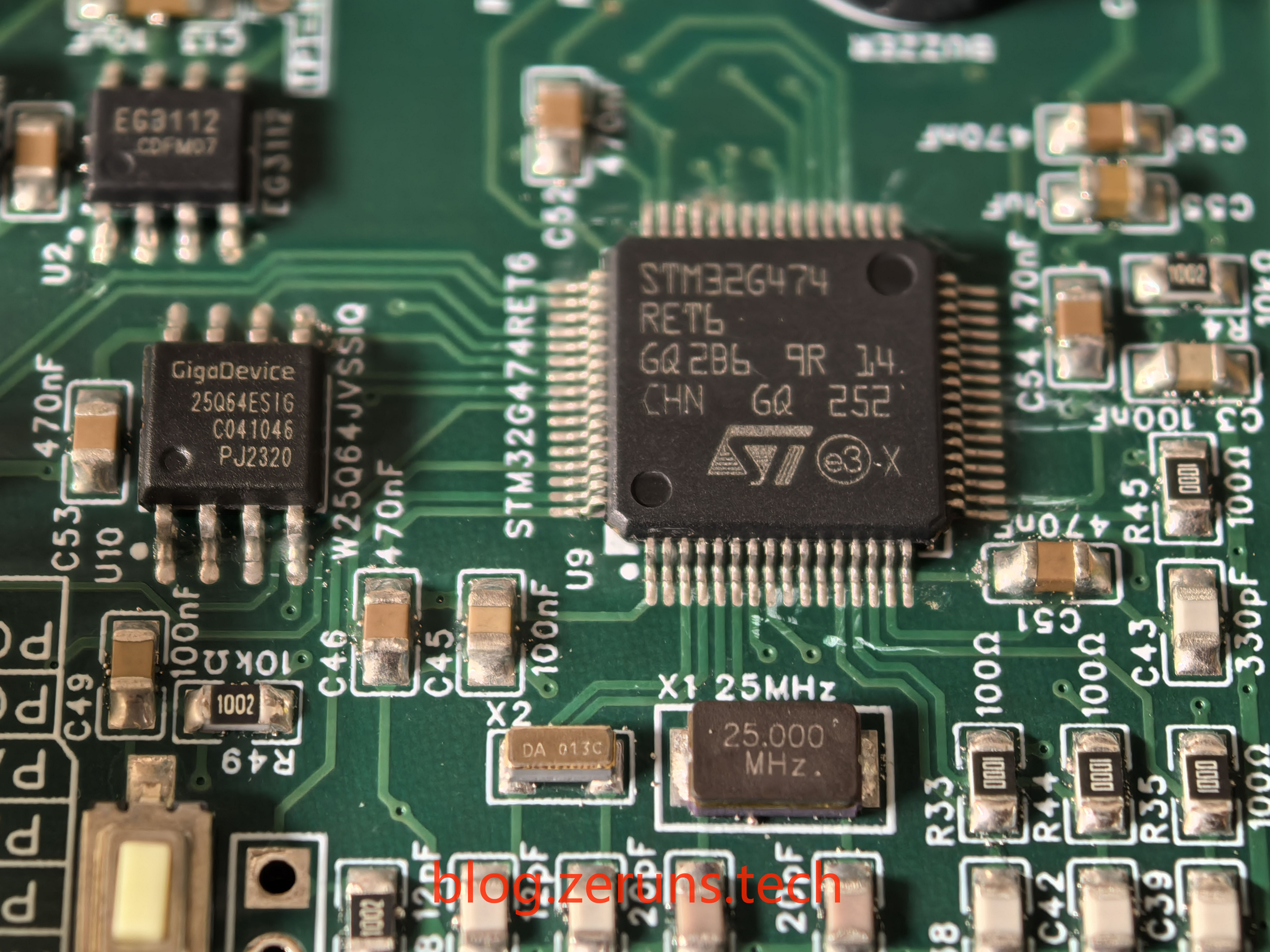
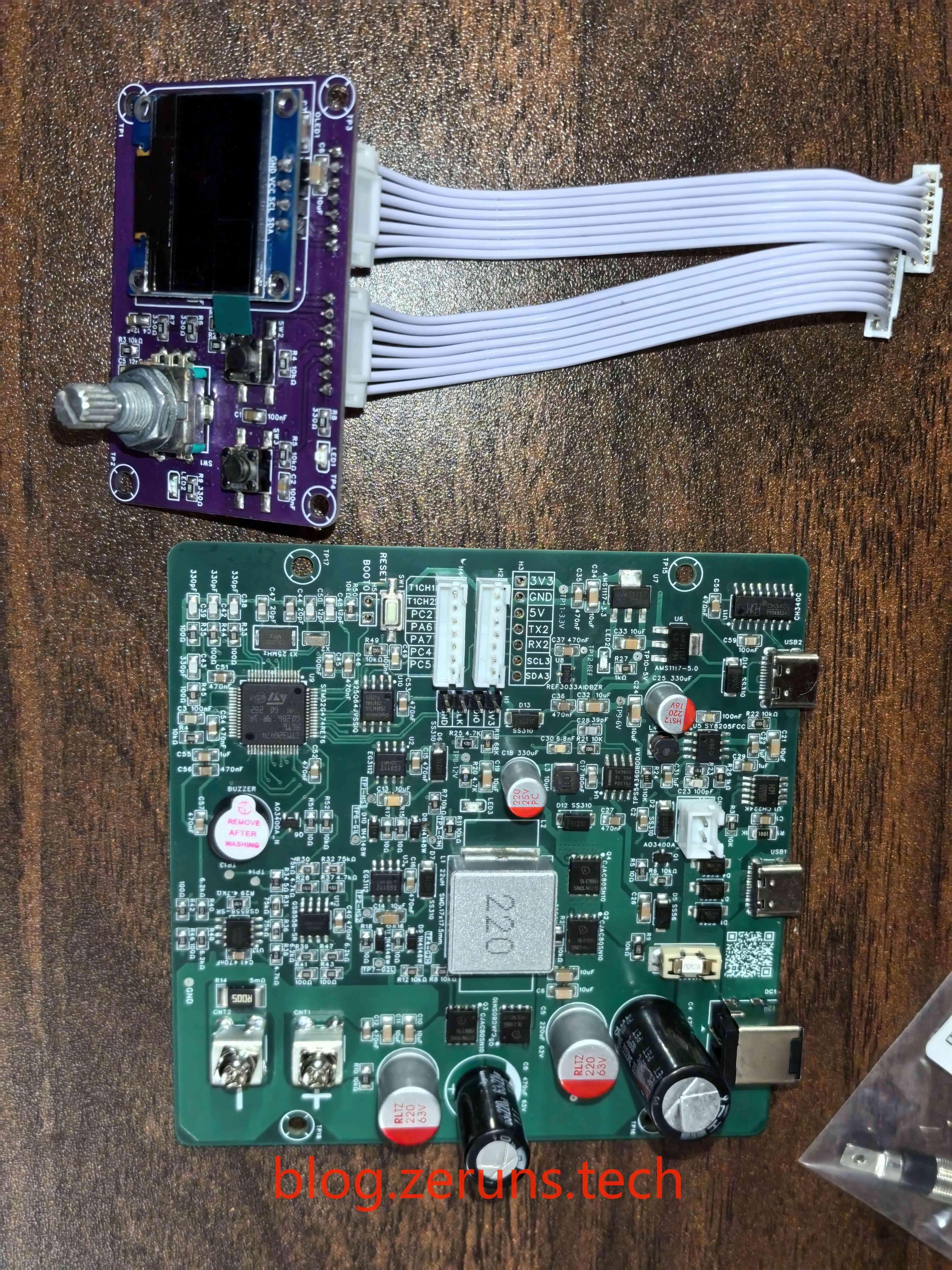
This digital power supply design uses the STM32G474RET6 chip as the controller. This controller has significant advantages such as simple peripheral circuits, diverse control methods, and excellent expandability. To achieve a precise clock signal, the controller uses an external crystal oscillator X1, a 25 MHz quartz crystal oscillator. In addition, the circuit includes multiple filter capacitors, including C45, C51, C56, C46, and C52, which are used on different digital power pins of the microcontroller (MCU) to ensure power stability and reduce noise interference. Resistor R49 and capacitor C49 constitute the power-on reset circuit, and SW1 is the MCU reset button. U11 is a USB-to-serial chip, model CH340C, connected to the second Type-C interface, and the serial port connects to the MCU's USART1 interface. U10 is a Flash memory chip, model W25Q64, used to store parameter settings and other information, and connects to the MCU's SPI3 interface. Q6 is the buzzer driver MOSFET, used to control the buzzer; the MOSFET gate is connected to the MCU's PB5 port. Terminal H1 is the SWD programming port. H2 and H4 are PH2.0 connectors for connecting to the control panel. The connectors have a reserved USART2 interface, allowing for easy replacement of the control panel with a serial port screen. An ESP32 can also be added to enhance networking and wireless control capabilities. D13 is a 5V reverse polarity protection diode. The schematic diagrams
of the cooling fan driver and motherboard temperature sampling
circuits are shown below. The power supply motherboard temperature sampling works by using an NTC thermistor R2 and a pull-down resistor R4 in series to divide the voltage and output it to the MCU's ADC port for sampling. The NTC thermistor used has a resistance of 10kΩ and a B value of 3950K.
The cooling fan is driven by an N-MOS transistor, model AO3400. A diode D2 is connected in reverse parallel to the cooling fan interface to prevent damage caused by the back electromotive force (back EMF) generated by the motor. When the motor is powered off, due to rotational inertia, the rotor will not immediately stop rotating but will continue to rotate and generate an electromotive force. This electromotive force can damage transistors or integrated circuits in a circuit, especially when the motor is connected to these components via semiconductor switches such as MOSFETs.
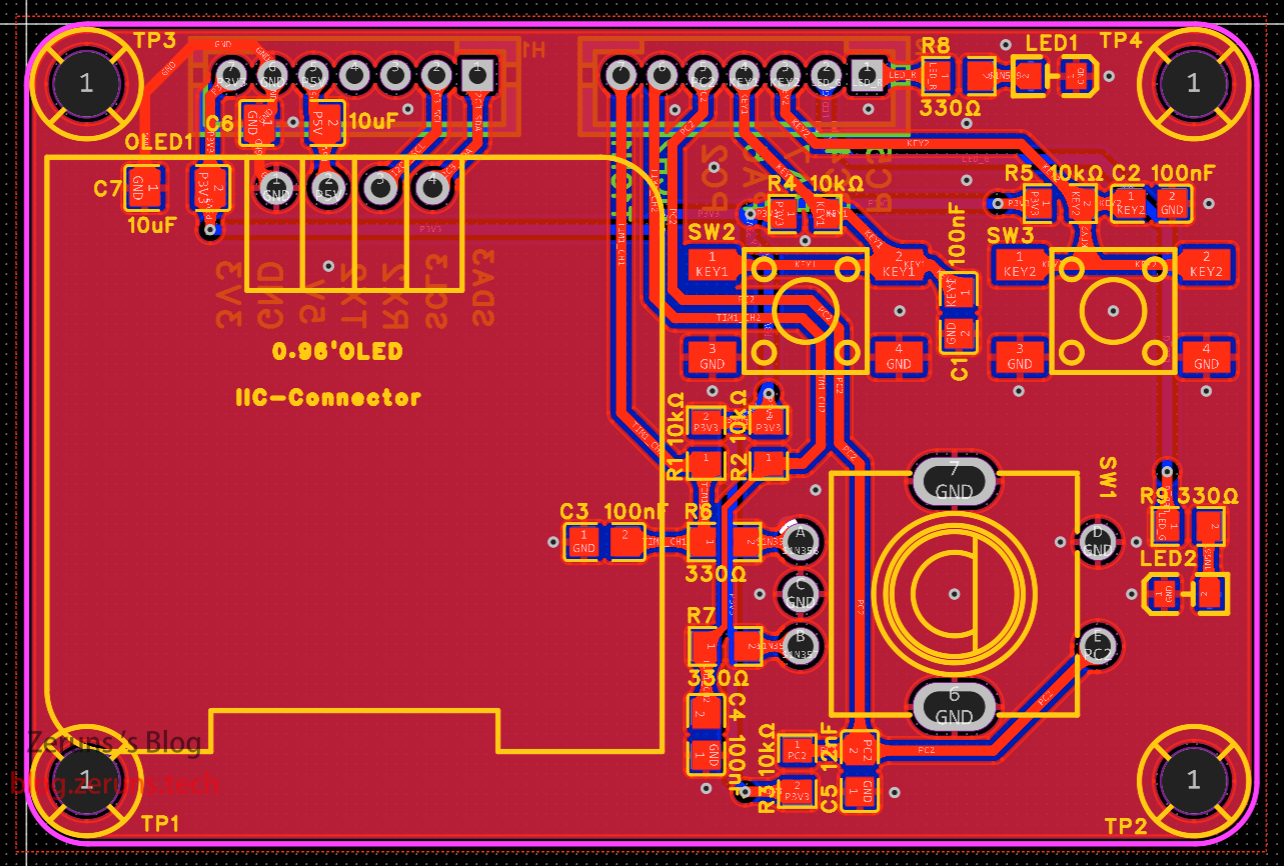
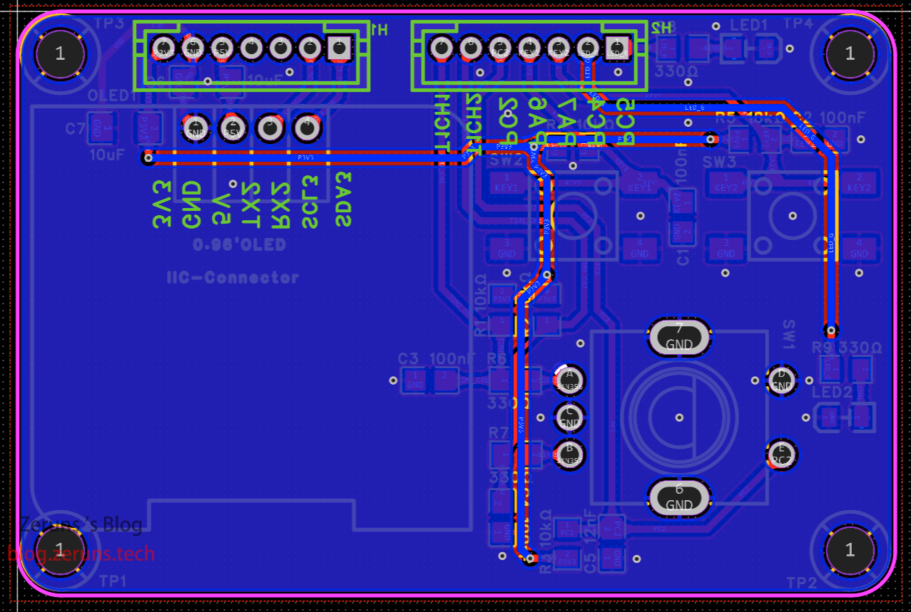
Control Panel Circuit Design
The circuit diagram of the control panel is shown below. SW1 is a rotary encoder used for setting parameters, etc. SW2 and SW3 are buttons; SW2 is used to switch settings, and SW3 is used to control the power output on and off. LED1 is the system running status indicator, flashing at 500ms intervals during normal operation. LED2 is the output status indicator, lit when the output is on and off when the output is off. OLED1 is an OLED screen used to display power parameters and status information.
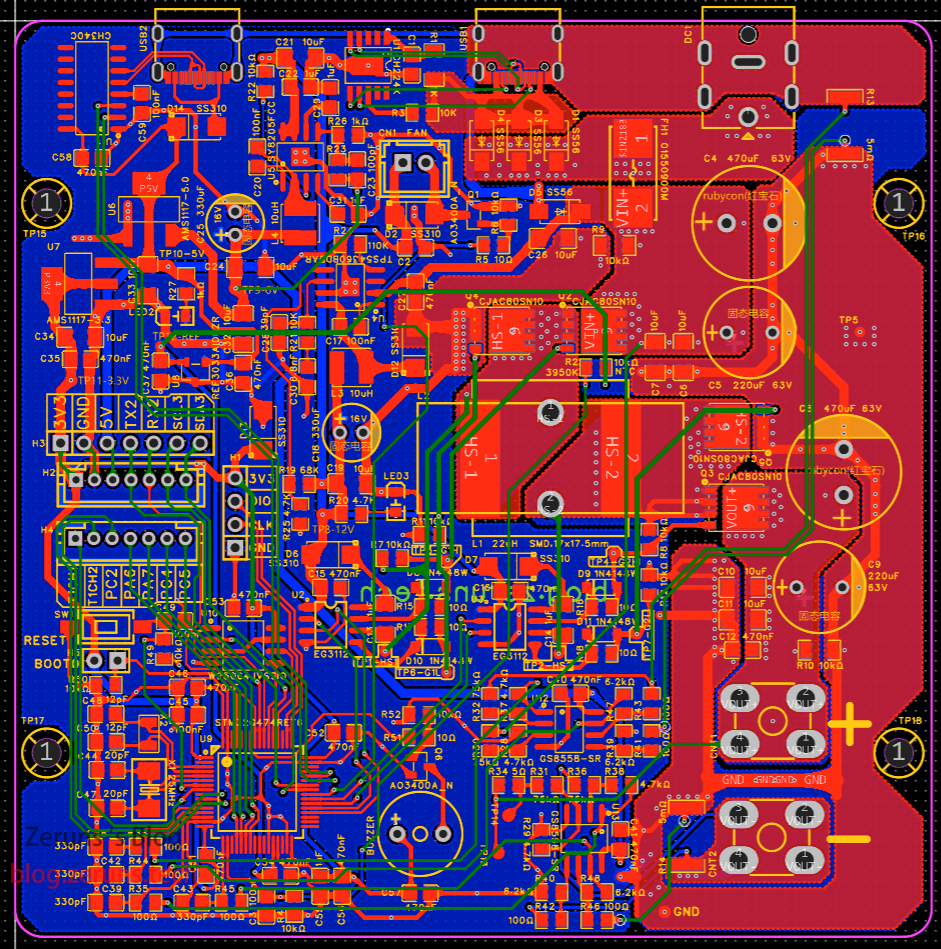
PCB Screenshot
Power Board Top Layer
Power Board GND Layer
Power Board Inner Layer 2
Power Board Bottom

Layer Top
Layer Bottom Layer
Instructions for Use
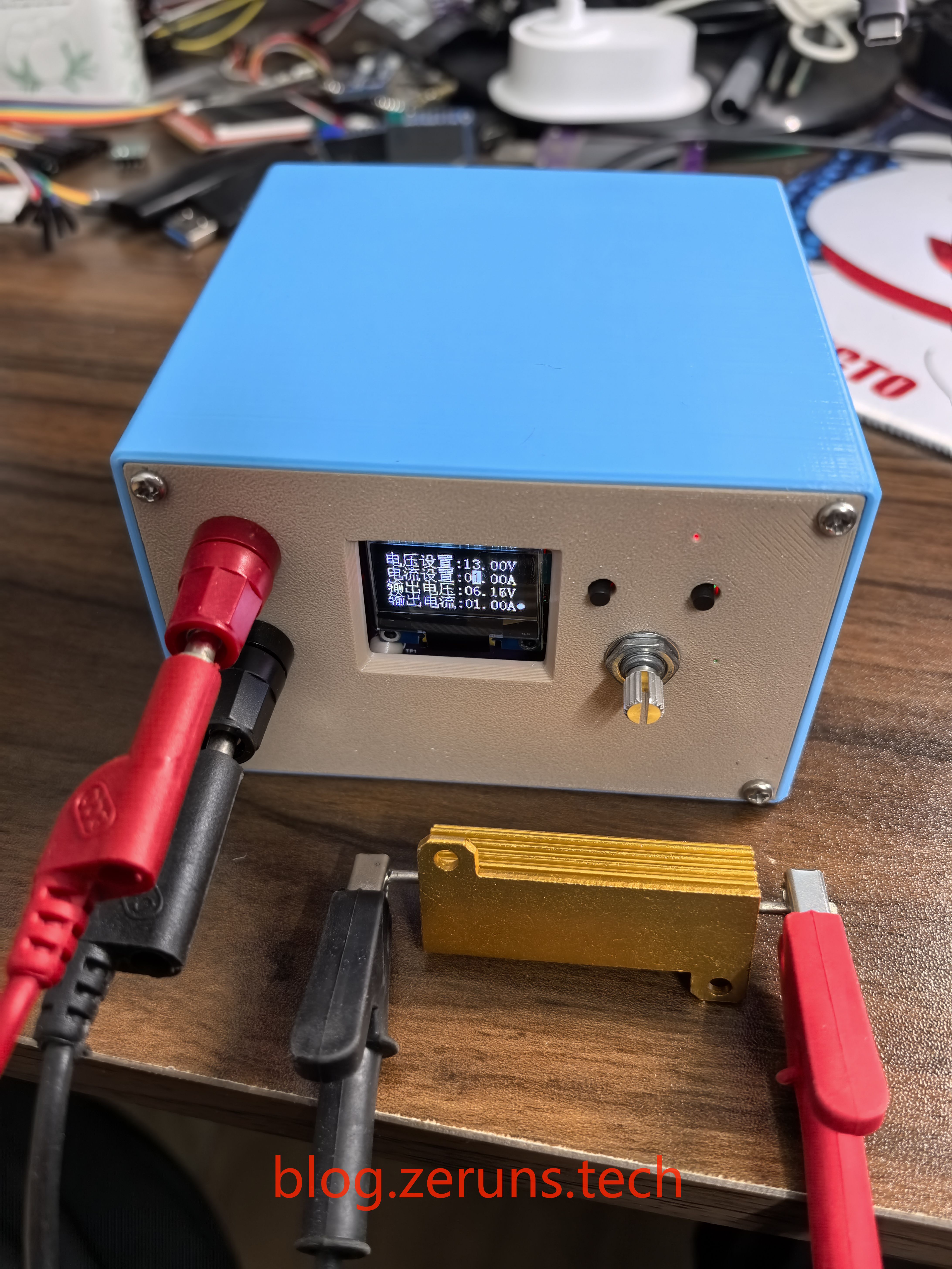
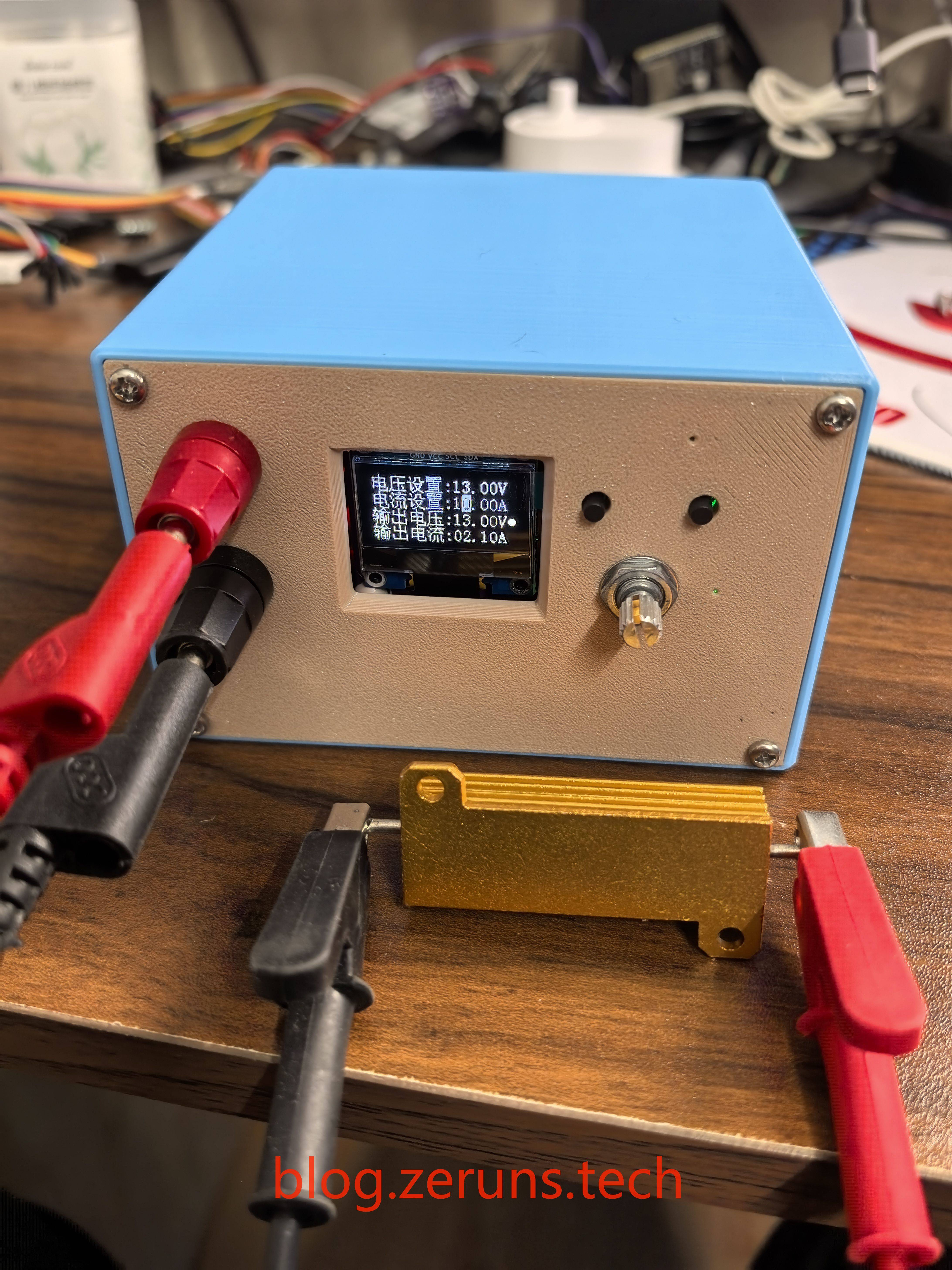
The output voltage and current values can be set using the buttons and rotary encoder. As shown in the diagram below, the inverted color display indicates the current setting position. The rotary encoder can be used to increase or decrease the value, and pressing the encoder switches to the next setting position. The SW2 button switches the setting item. The set data is automatically saved to the Flash memory chip, and the data is read from the memory chip the next time the system boots up.
SW3 button turns the power output on/off.
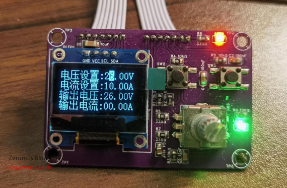
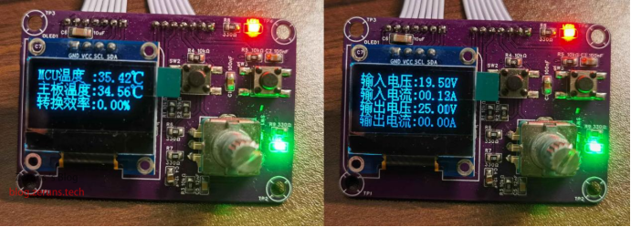
You can switch to the data display page to view the current input and output voltages and currents of the power supply, as well as information such as the motherboard temperature and MCU temperature, as shown in the figure below.
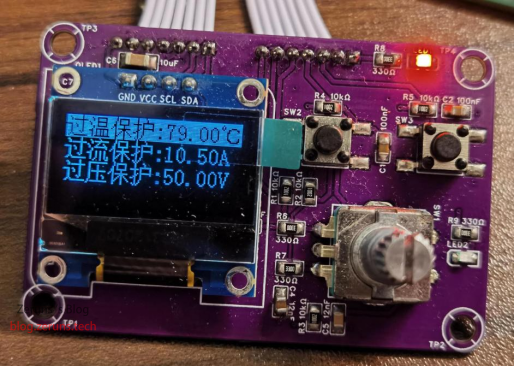
You can switch to the settings page to set the thresholds for over-temperature/over-current/over-voltage protection, as shown in the figure below. The set data is automatically saved to the Flash memory chip and will be read from the memory chip upon the next power-on.
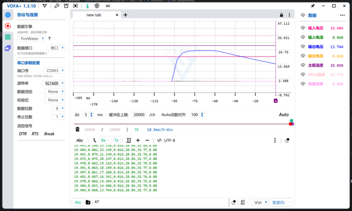
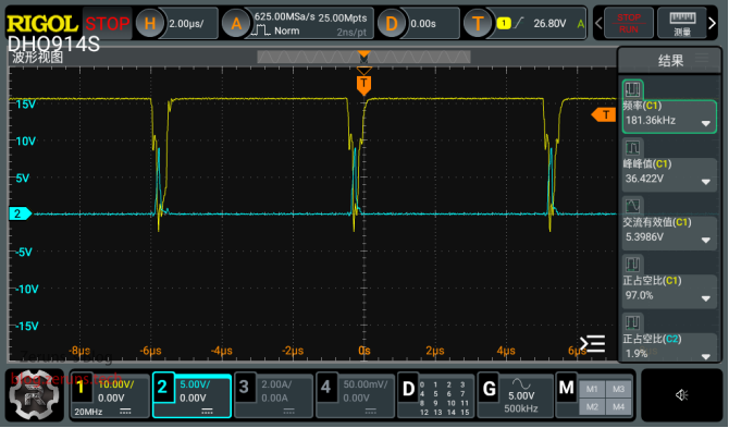
Ripple Test:
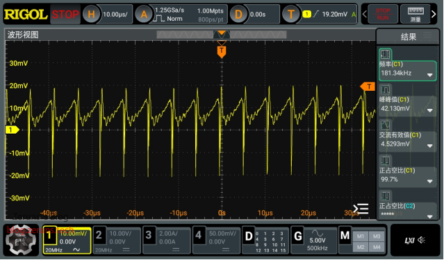
The power supply output performance and output ripple were tested using an electronic load and an oscilloscope, as shown in the figure below. At a 36V input and 12V 2A output, the peak-to-peak ripple was measured to be approximately 42mV, as shown in the figure below.
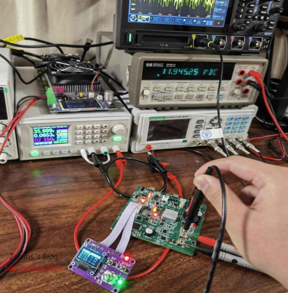
Conversion Efficiency Test
: The power supply conversion efficiency was tested at a 20V input and 12V 10A output, and was 92%, as shown in the figure below.
The table below shows the conversion efficiency at various input and output voltages, with the highest efficiency being 94.3%.
Input Voltage (V)
Input Current (A)
Input Power (W)
Output Voltage (V)
Output Current (A)
Output Power (W)
Conversion Efficiency (%)
20.003
4.035
80.712
15.010
5.000
75.050
92.985
47.999
5.335
256.075
24.040
9.900
237.996
92.940
48.000
7.875
378.000
36.020
9.900
356.598
94.338
48.000
9.860
473.280
45.030
9.900
445.797
94.193
23.998
8.835
212.022
48.070
4.000
192.280
90.689
23.998
9.830
235.900
35.998
6.001
216.024
91.574
12.099
9.166
110.899
24.070
4.000
96.280
86.817
20.008
2.645
52.921
4.970
9.000
44.730 84.522
20.008
10.550
211.084
24.030
8.000
192.240
91.073
36.000
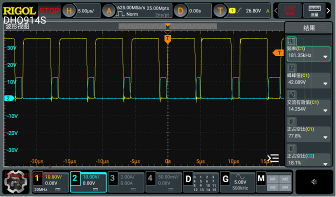
6.418 231.048 24.010 9.000 216.090 93.526 36.000 10.540 379.440 35.950 9.800 352.310 92.850 MOSFET gate waveforms . Tested the gate waveforms of various MOSFETs with 20V input and 24V output. Waveforms of the upper and lower transistors to ground in the BUCK circuit: Waveforms of the upper and lower transistors to ground in the BOOST circuit: Component Purchase Links Most of the components used in this project can be purchased here: 0805 resistors and capacitors sample book: https://s.click.taobao.com/begdskt STM32G474RE chip: https://s.click.taobao.com/C5yYWlt CH224K chip: https://s.click.taobao.com/4t4bskt CJAC80SN10 MOSFET: https://s.click.taobao.com/aPsWWlt EG3112 chip: https://s.click.taobao.com/1k9Zskt
220μF 63V Solid State Capacitor: https://s.click.taobao.com/n60Yskt
470μF 63V Rubycon Capacitor: https://s.click.taobao.com/WTRUWlt
GS8558 Op-Amp: https://s.click.taobao.com/usSVskt
TPS54360 Chip: https://s.click.taobao.com/r6lSWlt
SY8205 Chip: https://s.click.taobao.com/GxMUskt
AMS1117 Chip: https://s.click.taobao.com/mxASWlt
REF3033 Reference Chip: https://s.click.taobao.com/eOcTskt
W25Q64JVSSIQ Chip: https://s.click.taobao.com/QX7Tskt
CH340C Chip: https://s.click.taobao.com/QYRQWlt
3.3V Active Buzzer: https://s.click.taobao.com/sovPWlt
Type-C Female 16P: https://s.click.taobao.com/vjLRskt
It is recommended to purchase components from LCSC Online Store: https://activity.szlcsc.com/invite/D03E5B9CEAAE70A4.html
Click on the BOM in the LCSC open-source link to immediately place an order on the LCSC Online Store; you can import the required components into your shopping cart with one click.
Download
links below contain: LCSC EDA project, schematic PDF files, datasheets for various chips, source code project compressed package, and some reference program code.
Download links: 123 Cloud Drive (unlimited speed): https://www.123pan.com/ps/2Y9Djv-8yevH.html
Baidu Cloud Drive download link: https://url.zeruns.tech/MW2d1
Project program Gitee open-source address: https://gitee.com/zeruns/STM32-Buck-Boost
Project program GitHub open-source address: https://github.com/zeruns/Synchronous-Rectification-Buck-Boost-Digital-Power-Supply-Based-on-STM32
Please give it a star and a like.
Known issues:
The SY8205 chip in the auxiliary power supply enters PFM mode at low loads, resulting in a low frequency and slight noise. The
PID control program for constant current mode is poorly written; it is only stable under purely resistive loads. (Constant voltage mode works fine.)
Other recommended open-source projects
include: a three-phase power acquisition device for easy monitoring of home electricity usage: https://blog.zeruns.tech/archives/771.html;
an LVGL project template based on STM32F407 (MSP3526 screen), including FreeRTOS and bare-metal versions: https://blog.zeruns.tech/archives/788.html;
the Qinheng CH32V307VCT6 minimum system board open source: https://blog.zeruns.tech/archives/726.html;
and the LM25118 automatic buck-boost adjustable DC-DC power module: https://blog.zeruns.tech/archives/727.html
EG1164 high-power synchronous rectification boost module open source, with a maximum efficiency of 97%: https://blog.zeruns.tech/archives/730.html
4G environmental monitoring node based on ZTE Air700E (data on temperature, humidity, air pressure, etc.), uploading to Alibaba Cloud IoT platform via MQTT: https://blog.zeruns.tech/archives/747.html
Smart electronic load based on HT32F52352 open source, a project from the Holtek Cup open source: https://blog.zeruns.tech/archives/784.html


 京公网安备 11010802033920号

 S3S12G128F0VTJR


