Project Description:
Visible light cameras offer high resolution and frame rate, while thermal imaging sensors measure temperature distribution but suffer from low resolution and frame rate. Visible light images are used to compensate for thermal imaging images, resulting in higher-quality heat distribution maps. The device itself contains a standard visible light camera and a thermal imaging sensor. After being read by the MCU, the data is transmitted to a mobile device via USB. The mobile device's powerful computing capabilities enable image processing and fusion, displaying the final image on the phone screen. The software is licensed under the MIT
license
, granting the licensee the right to use, copy, modify, merge, publish, distribute, sublicense, and sell the software and copies thereof. Licensees may modify the license terms as needed for the program. Copyright and license notices must be included in the software and all copies thereof, but the original author assumes no risk of use and has no obligation to provide technical support.
Project-related functions:
The overall functional framework of this project is as follows: The MCU reads thermal imaging sensor data via the I2C interface and then transmits it to a USB hub via the USB interface. The camera is a universal driverless USB camera, also connected to the USB hub. The USB hub connects to an Android phone. The Android phone has two devices: one is the camera, and the other is the thermal imaging sensor. The Android phone application layer obtains data from both sensors, fuses it using a certain algorithm, and obtains a high-resolution, high-quality thermal image.

Project attributes:
This project is being publicly disclosed for the first time and is my original work. This project has not won any awards in other competitions.
Project Progress
20231128:
Basic functions are OK, but completion still needs further optimization. Known issues are as follows:
The STM32 USB to SL2.1A line connection is reversed. This has been corrected in the project
; images in scenes with excessive brightness will be overexposed
. Screen rotation is not currently adapted; please turn off screen rotation. 20240203:
Added high and low temperature tracking, algorithm parameter adjustment, fusion mode switching, and frame rate switching functions.
Optimized the interface, fixed some bugs, and automatically locked screen rotation.
Added 3D printed shell design principle.
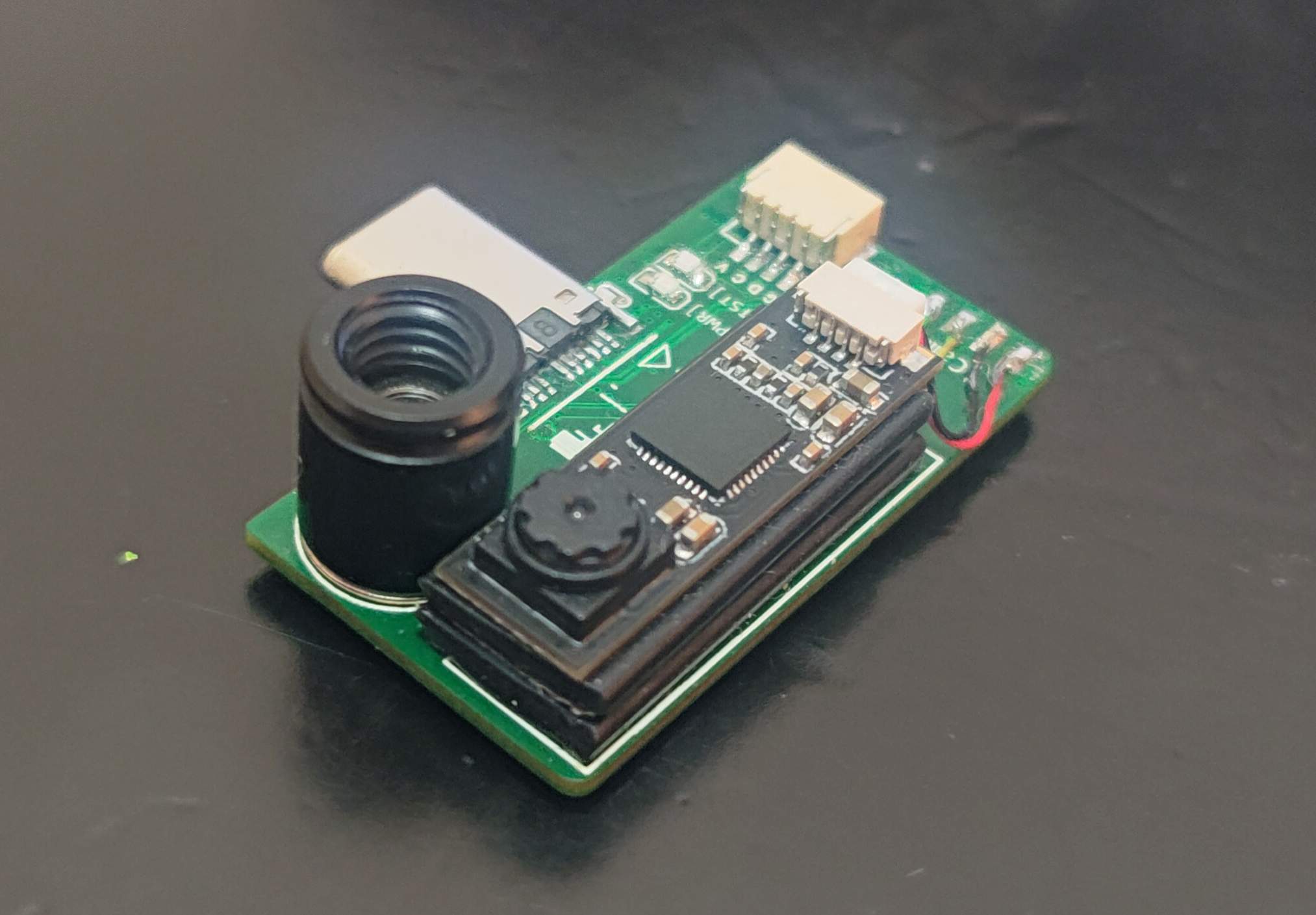
MCU
: The MCU uses STM32F411CEU6, with a floating-point unit that can process thermal imaging data. It has USB FS. The minimum system circuit is as follows.

USB Hub:
The USB Hub uses SL2.1A and supports USB HS, which can be used to transmit camera data. According to the manual, a crystal oscillator U3 is connected here and does not need to be soldered. USB1 is a USB Type-C male connector used to connect to a mobile phone.

The camera uses a 640x480 UVC camera daughterboard, which is soldered to the CAM_DM/CAM_DP
thermal imaging sensor.
The thermal imaging sensor uses an MLX90640 with a resolution of 32x24 pixels and an I2C interface with a maximum speed of 1MHz.

The power supply
uses an LDO for voltage regulation, model ME6211, which can directly use low-ESR ceramic capacitors for input and output voltage regulation.

Other
power supplies include LEDs and test LEDs .

The SWD interface

test points are debugged, and the firmware uses UART2 as the debug serial port.

The software documentation and
code resources
are divided into three parts: single-board firmware, Android App, and 3D printed shell. Single
-board firmware :
https://github.com/colourfate/thermal_bridge
Android App:
https://github.com/colourfate/ThermalEyes
3D printed shell
: Download 3d_printed_casing.zip from the attachment. The document provides STEP and STL files for direct printing
of the single-board firmware
development environment.
Currently, the STM32CubeIDE
software workflow is used
. The software consists of two parts: the MLX90640 driver and the thermal imaging data transmission protocol. In general, the software workflow involves reading data from the MLX90640 via I2C, packaging it, and finally sending it via USB. The entire process can be completed in a single loop. The MLX90640's temperature measurement range is -40 to 300 degrees Celsius, rounded to two decimal places and converted to an integer of -4000 to 3000 degrees Celsius. 000, can be overridden with a 16-bit integer . The official mlx90640

driver
is already provided; you only need to implement the corresponding I2C read/write operations to read sensor data via API.
The data protocol:
Data acquired from the sensor needs to be sent via USB. Since the acquired temperature is of float type, only two decimal places are needed for accuracy; therefore, converting it to an integer saves bandwidth. The mlx90640 temperature measurement range is -40 to 300 degrees Celsius, and a 16-bit signed integer can be used. The communication protocol with the host computer is as follows:
----------------------------------------------------------------------------
| header | type | length | data[0] | data[1] | ... | data[n] |
----------------------------------------------------------------------------
header: uint16_t, start code, fixed at 0x8000
type: uint16_t, indicating data type
length: uint16_t, indicating data packet length, indicating the number of subsequent data packets
data: uint8_t array, containing actual data USB Sending
The USB library is automatically generated by CubeIDE, and you can directly call USBCDC to send data
Android APP
There are two USB devices here, one is a USB serial port, used to transmit thermal imaging data, and the other is a USB camera, used to transmit image data. The Android side mainly completes the data reading, fusion and display functions
Software Framework
Both Camera and thermal imaging sensor data reading have corresponding libraries to support them. Both libraries use asynchronous callback for data reading, so a double buffer caching mechanism is used here. Taking Camera as an example:
initialize a queue of length 2. When the callback occurs, allocate a new buffer, copy the YUV data into this buffer, and then put this buffer into the queue.
A thread is started to continuously read data from the queue for data fusion.
If the thread reads too slowly, the callback will find that the queue is full, so it will take a buffer from the queue and discard it, and then put a new buffer into the queue.
If the callback never comes, the thread will find that the queue is empty and will skip the next read.
Because a new buffer is allocated for each callback, there is no concurrency problem with the buffer.
Adding and deleting data from the queue accesses the same data structure, which has a concurrency problem. Locking is required during operation.
As mentioned above, there are two queues, one for YUV data and one for thermal imaging data. A thread accesses both queues. Data is taken out only when both queues have data for data fusion. In summary, the overall software flow is as follows:

Android supports cameras using UVCAndroid. Reference article: https://blog.csdn.net/hanshiying007/article/details/124118486
This library is based on saki4510t/UVCCamera and provides a simpler interface. For previewing and data reading, refer to the CallbackDemo. You need to override ICameraHelper.StateCallbackd. Here, the camera data is retrieved and placed into a YUV queue. The format is as described in NV21
thermal imaging data reading and preview
3.2. The thermal imaging data is transmitted via USBCDC. On the Android side, it appears as a virtual serial port. In the Android development environment, felHR85/UsbSerial is used to provide virtual serial port operation support. In the callback, the thermal imaging data is placed into the queue.
Data fusion and
data acquisition
use a single thread to retrieve data. Here, the camera frame rate is expected to be higher than the thermal imaging frame rate. Data fusion is only performed when there is data in the mYUVQueue queue. When there is no data in the mThermalQueue, the data
fusion algorithm
of the previous frame is used. Here, the camera captures a visible light image with a resolution of 640x480, while the thermal imaging captures the temperature distribution with a resolution of 32x24. The purpose of the fusion algorithm is to use the visible light image as a reference to give the thermal imaging temperature image more detail.
The first step of the fusion algorithm is to extract high-frequency information from the visible light camera. Since the current Android app integrates OpenCV, the previous method is no longer used. Here, Gaussian blur is used to extract high-frequency information. Refer to the blog: Using OpenCV Mat to extract and losslessly restore low-frequency and high-frequency information from images (Gaussian blur, subtraction, summation).
`Mat im_cam_l;
GaussianBlur(im_cam, im_cam_l, Size(11, 11), 5, 5);
Mat im_cam_h = im_cam - im_cam_l;`
After extracting the high-frequency information, it is superimposed on the interpolated and enlarged thermal imaging image to obtain the fused image. Finally, pseudo-color is applied.
`Mat im_fusion = im_cam_h + im_them_scale;
applyColorMap(im_fusion, im_fusion_color, ...;` The simulation results are as follows (COLORMAP_JET).
The first image is taken by the camera, and the second image is an image of the temperature distribution obtained from thermal imaging after interpolation and magnification. Both images have a resolution of 640x480.


First, high-frequency information is extracted from the visible light camera. The low-frequency and high-frequency information are as follows.


Then, the thermal imaging image is superimposed and assigned pseudo-color using the JET color table. The result is as follows.

Color mapping
: Color mapping directly assigns pseudo-color to the thermal imaging image and then superimposes it onto the visible light image in a YUV manner. Since the visible light image itself contains a large amount of information, it is equivalent to increasing the amount of information in the thermal imaging. The basic idea of color mapping is to convert the RGB components of the thermal imaging into YUV components according to the formula, and then subtract 128 from each as the offset of the visible light image before superimposing it onto the visible light image. The color mapping effect is as follows.

Design Notes:
1. U3 ferrite beads are for testing purposes only and do not require soldering! No soldering required! No soldering required!
The USB cable from STM32 to SL2.1A was reversed. After correcting with a jumper wire, it was verified to be working correctly. This has been fixed in the project, but due to time constraints, it hasn't been prototyped yet. If you're unsure, you can revert to the first prototype version (release_1) in version control and then correct it yourself

. 3. The prototype thickness of the board in the demonstration is 1.2mm.
4. The camera's USB speed is high, so impedance control is needed during prototyping .
5. Refer to this link for the camera daughterboard; the connection wire spacing is 0.8mm. Refer to this link as well


. 6. The MLX90640 sensor is relatively tall; it's best to elevate the camera daughterboard slightly. The following are earlier version
demonstration
videos on Bilibili : https://www.bilibili.com/video/BV1M64y177ig Principle explanation: https://www.bilibili.com/video/BV1yb4y1T7hD Single board hardware shooting effect , color mapping effect, image fusion effect.


202311241743.mp4
202311241819.mp4
thermal_bridge-main.zip
ThermalEyes-main.zip
3d_printed_casing.zip
PDF_Binocular Mobile Thermal Imaging Device.zip
Altium binocular mobile thermal imager.zip
PADS_Binocular Mobile Thermal Imaging Device.zip
BOM_Binocular Mobile Thermal Imaging Device.xlsx
90980
High-speed wireless DAP debugger Lite
A high-performance, low-cost wireless DAP debugger based on the ESP32-S3, with a BOM cost of only 30 yuan and wireless speeds approaching those of the STLink V2.
This project is prohibited from commercial use without authorization
. Authorized sales are available through Taobao-ABrobot Smart and Taobao-Tacker Innovation.
Two open-source wireless debuggers have been released, which you can choose based on cost and usage environment:
CH32 version: Cost approximately 100 RMB, under test conditions, 98KB/s wired download speed, 48KB/s wireless download speed, strong anti-WiFi interference capability, compatible with lower Keil versions :
https://oshwhub.com/ylj2000/dap_hs_wl_v0-4
ESP32 version: Cost approximately 30-40 RMB, under test conditions, 94KB/s wired download speed, 43KB/s wireless download speed, moderate anti-WiFi interference capability; poor WiFi environment may cause download speed reduction or even download failure, but it has little impact on normal personal use, only a greater impact in environments such as competition venues, Keil version higher than 5.29 is required.
https://oshwhub.com/ylj2000/dap_hs_esp_open
Update Log
#2023.09.13
Updated module version and corresponding shell
#2023.09.01
Initial Release
I. Introduction
Usage Environment: MDK>=5.29, IAR>=8.32. The main chip only requires two ESP32-S3FN8 or ESP32-S3FH4R2 chips, with a BOM cost of around 30 RMB. Ready-made modules can also be used. Wireless performance is approximately twice that of common wired FS+HID DAPs, and even close to wired STLink V2. The distance can reach over 30m (further distances have not been tested, but there is no significant speed attenuation).
A wireless debugger consists of a transmitter (Host) and a receiver (Slave). The hardware and software at both ends are completely identical. Pairing, mode switching, and wireless channel adjustment can be performed via buttons. Like regular DAPs, it supports debugging ARM microcontrollers (such as STM32, GD32, etc.), supports SWD and JTAG, hardware and software resets, and virtual serial ports. After pairing, it's plug-and-play, requiring no driver installation (WIN10 and above); it doesn't use WiFi, but rather a 2.4G-like wireless connection, so there's no need to wait for a wireless connection. Besides wireless mode, it can also be switched to wired mode (USB) for use in complex wireless environments, where performance is better. Different indicator light colors represent different modes: red for wired mode (USB), blue for wireless transmitter (Host), and green for wireless receiver (Slave).
II. Development Background
Currently, commonly used debuggers for ARM microcontrollers include ST-Link, J-Link, and DAPLink. Although their functions and speeds differ, almost all of them can only be used with a USB cable. This can easily damage the computer or even injure the user in some potentially dangerous debugging tasks, such as with robots or power supplies. Wireless debuggers can effectively avoid these situations and greatly optimize the debugging experience, eliminating the need to carry a computer and USB cable around with the target.
Most wireless debuggers on the market, like DAPLink, are based on the CMSIS-DAP protocol. However, their performance and price vary greatly. Many offer extremely low costs and poor performance at exorbitant prices, making them very difficult to use and causing many developers, including myself, to make mistakes. I've tried many wireless debuggers, and the only one that was relatively good was the one from Zhengdian Atom, but its price was too high (300+ RMB), making it unaffordable. Therefore, I decided to DIY a good and inexpensive wireless debugger. In my previous open-source project, I developed one based on CH32V307+SX1281, costing less than 100 RMB, but with performance comparable to Zhengdian Atom. However, the cost was still relatively high, so I planned to develop a cheaper wireless debugger that still met general usage requirements.
The performance of the previous version was approximately: MDK+STM32F4, program speed 98KB/s wired, 48KB/s wireless. The initial target speed for this version was: wired speeds close to the previous version, and wireless speeds around 30KB/s. To achieve this, HID mode DAP was not feasible, so a WinUSB-based Bulk mode was necessary. For cost reasons, choosing a microcontroller with built-in USB and wireless capabilities was essential. Initially, the ESP32-S2 and ESP32-S3 were considered, but in subsequent tests, the ESP32-S2's TinyUSB consumed too much CPU resources, resulting in wired speeds only reaching 40+ KB/s; while the ESP32-S3, being a dual-core design, achieved wired speeds exceeding 90KB/s after task allocation to both cores. Therefore, despite the higher price of the S3, the ESP32-S3 was chosen.
After hardware design and software optimization, the final performance even exceeded the initial design goals, reaching speeds very close to the previous version's 100-yuan configuration, while the cost of this version was only about 30 yuan. Program speeds were 95KB/s wired and a maximum of around 45KB/s wirelessly. Of course, since ESP uses a WiFi channel, the actual speed may decrease depending on the wireless environment, but it is generally around 40KB/s. This performance is very close to that of the Zhengdian Atom wireless debugger. At one-tenth the price, what more could you ask for?
III. Finished Product Showcase

III. Manufacturing Process
1. PCB Fabrication: Fabricate the PCB according to the open-source documentation, selecting a 1.0mm board thickness.
2. PCB Soldering: Most of the components used can be purchased from LCSC, or you can find cheaper options on Taobao. The attached BOM contains reference purchase links; it is recommended to choose according to your needs.
3. Firmware Download: After confirming the PCBA fabrication is correct, download the debugger firmware. Press and hold button A while connecting the debugger to the computer via USB cable. Open the flash_download_tool in the attachment and select the following configuration. After entering the interface, select firmware, set the starting address to 0, and select the corresponding serial port. It is recommended to first click ERASE to erase the Flash, and then click START to burn. After burning, power on again; the default mode is USB (indicator light is red).

4. Pairing: For the first module, press and hold button B to power on until the indicator light turns purple, then release. The second module is powered on by pressing and holding button B. After the indicator light turns purple, the two modules will instantly transform into master (blue) and slave (green) respectively. At this point, the communication parameters and modes at both ends are automatically set. These can be changed using the buttons if needed. The master and slave modules need to be powered on again after completion.
5. Button Function Setting Mode: Press and hold button A until the indicator light turns yellow. Short press button B to adjust to the desired mode based on the indicator light color. If you need to save the configuration to Flash, i.e., retain the current configuration upon next power-on, press and hold button A until the indicator light flashes yellow, then short press button A to exit. If it's only for temporary use and you don't need to save the configuration to Flash, simply short press button A to exit. Setting the Wireless Channel: Press and hold button B until the indicator light flashes. The flashing color and number of flashes indicate the current WiFi channel: green for channels 1-5, red for channels 6-10, and blue for channels 11-13. Short press button B to select the target channel, then press and hold button A until the indicator light flashes yellow, then short press button A to exit. The master and slave devices need to be configured to the same channel to communicate. After completion, both the master and slave devices need to be powered on again.
6. Testing: Test whether the download, virtual serial port, and other functions are normal.
IV. Daily Use
1. Keil Settings
If you encounter connection failures or unstable connections, you can try lowering the clock frequency and replacing the DuPont wires. In addition, some chip models may not be able to be debugged properly at high clock frequencies (the HK32F030MF4P6 I used is an example).


2. Interference:
If you encounter severe signal interference on the current wireless channel, try changing to a different communication channel. Excessive interference can lead to reduced speed and unstable downloads.
V. Performance Testing
Environment: Keil MDK 5.34
Target Chip: STM32F407VGT6
Firmware Size: Approximately 1024K
Testing Method: Timed with a stopwatch on a mobile phone, averaging three tests.

Since the Erase and Verify times are roughly the same for each downloader, the Program duration and speed, which reflect the downloader's download speed, are calculated.
In the table, CH32V307 is the previous version, and ESP32-S3 is this version. As you can see, this version of the debugger's performance is very close to the previous version. The wired mode speed slightly exceeds Jlink V9, while the wireless mode speed is slightly lower than STLink V2. I've also tested some wireless debuggers on Taobao, many of which have speeds of only a few tens of KB/s, which is normal, as the speed of a typical wired DAP is only 20+ KB/s.
For more information, please join QQ group: 770979540 for discussion.
BOM.xlsx
flash_download_tool_3.9.5_0.zip
Top and bottom cover drawings.dwg
Module version shell.7z
DAP_HS_ESP_20231027.bin
PDF_High-Speed Wireless DAP Debugger Lite.zip
Altium_High-Speed Wireless DAP Debugger Lite.zip
PADS_High-Speed Wireless DAP Debugger Lite.zip
BOM_High-speed wireless DAP debugger Lite.xlsx
90981
Based on the Liangshan School's self-balancing O-type wheelbarrow
The unicycle model in this project uses the O-model provided in the 18th Intelligent Vehicle Competition, and is designed with the Jialichuang Liangshanpai as the main control board, enabling it to complete the tasks in the 18th Intelligent Vehicle Competition.
Project Description:
This project uses the O-model unicycle provided in the 18th National Intelligent Vehicle Competition. It is designed using the JLCIC Liangshanpai main control board and can complete the tasks from the 18th National Intelligent Vehicle Competition (code is attached).

Open Source License: GPL 3.0 Project Functions
: 1. Unicycle structure, using one bottom wheel motor and two momentum wheel brushless motors. A 6s battery is used. 2. A DRV8701 is used as the brushed motor driver for the bottom wheel, and the motor's forward and reverse rotation and speed adjustment can be controlled via PWM. The brushless motor has its own driver and does not require additional drive . 3. Tracking can be achieved by sensing electromagnetic signals, similar to the method used in the National Undergraduate Intelligent Vehicle Competition. 4. A Bluetooth interface is reserved on the main control expansion board for easy communication with mobile phones, and a DAPlink interface is provided for easy downloading and plugging/unplugging. 5. The power board has a reverse connection protection circuit, one 5V power supply and two 3.3V power supplies, and one DRV8701 full-bridge motor driver . For safety, the power supply section is isolated from the core board. Note: This section describes the overall functionality of the project. Project Attributes : This project is being publicly disclosed for the first time and is my original work. The project won second prize in Shandong Province at the 18th Intelligent Vehicle Competition. This project is being publicly disclosed for the first time and is my original work. The project has not won any awards in other competitions. Project Progress: Overall project progress, application for project consumables costs. 9. Required! 2023-08-08 Project awarded; design scheme started on August 25, 2023; software scheme design completed on September 28, 2023; first version of hardware scheme completed on October 5, 2023; first version of hardware received and tested on October 15, 2023; second version of hardware design completed on October 18, 2023; second version of hardware received and tested on October 25, 2023; hardware testing completed and debugging started on November 14, 2023; basic tasks completed, video recorded on November 20, 2023; first shipment sent for testing and acceptance, and rectification completed on December 22, 2023; second shipment sent for testing and acceptance, and rectification completed on January 15, 2024; second shipment sent for testing and acceptance completed. And rectification design principle prompts: Design principle description of this project Model introduction 1.1.1 The main body of the model is 215mm long, 356mm high, and 116mm at its widest point. The whole car is made of anodized alloy. The double flywheel structure can stand in balance and can also turn freely . Purchase link: https://item.taobao.com/item.htm?abbucket=18&id=701275309058&ns=1&spm=a21n57.1.0.0.3332523c9gQgpf&skuId=4944447208762 1.1.2 The official brushless motor is a Nidec O-1104 DC brushless motor (DC24V, speed 6000r) used to control the rotation of the momentum wheel. The motor features a built-in brushless drive with a 100-line dual-channel encoder, suitable for high-precision feedback control. It supports PWM signal speed regulation and forward/reverse rotation, includes an emergency stop function, and supports forward/reverse switching and stepless speed regulation. Purchase link (the motor is included with the complete vehicle purchase; it doesn't need to be purchased separately, but can be considered for replacement parts): https://item.taobao.com/item.htm?abbucket=18&id=716033359390&ns=1&spm=a21n57.1.0.0.76f5523cDrhemB&skuId=5000259636337 1.1.3 DC brushed motor ( DC7.2V, 800rpm) provides strong support for the model car to complete competition tasks. Purchase Link: https://item.taobao.com/item.htm?abbucket=18&id=693298985042&ns=1&spm=a21n57.1.0.0.76f5523cDrhemB 1.1.4 The unicycle wheel has a diameter of 54mm and a width of 16mm. The rim is made of anodized alloy, and the exterior is made of environmentally friendly TPR material with a pattern, providing high friction and making it sturdy and impact-resistant. Other accessories are listed in the attached table. Control Principle: The unicycle control algorithm can be broadly divided into two parts: balance control and tracking control. Its overall anti-interference capability and response speed are important indicators for evaluating the overall performance of the unicycle. Balance Part: The front and rear balance of the unicycle is controlled by the bottom wheel. The algorithm uses a three-loop cascade PID to control its front and rear tilt angles, keeping it stable overall. The left and right balance of the unicycle is controlled by the front and rear momentum wheels. The algorithm also uses a three-loop cascade PID to control its left and right tilt angles, keeping it stable overall. The unicycle's balance control relies on a momentum wheel and uses cascaded PID control. This requires connecting three PID controllers in series: an angular velocity loop, an angle loop, and a speed loop. Based on response time, the angular velocity loop is the innermost loop, followed by the angle loop, and the speed loop is the outermost loop, similar to upright bikes and balance bikes. The code implementation of cascaded PID is relatively simple, and the concept is easy to implement: connecting three ordinary PID controllers in series and using different control cycles to achieve cascaded PID. However, the error input physical quantity of each PID is different, and the input of the inner loop PID must be related to the output of the previous loop PID. For the tracking section: the electromagnetic acquisition circuit is a necessary sensor for the intelligent vehicle to continue driving when the circuit is broken. The electromagnetic acquisition circuit consists of frequency selection, amplification, and detection, providing the microcontroller with a stable voltage induced by the energized enameled wire in the middle to determine the vehicle's position. Through Professor Zhuo's articles on signal and demodulation, we learned about signal-related knowledge and selected an operational amplifier and detector circuit as the electromagnetic acquisition circuit according to the electromagnetic vehicle guide published by the competition organizing committee. This circuit can simultaneously amplify and detect signals, resulting in low output impedance. For a straight conductor, when the cart, equipped with two coils symmetrical about its central axis, travels along the conductor, the induced electromotive forces (EMFs) in both coils should be the same in magnitude and direction. If the cart deviates from the conductor, meaning the two coils are asymmetrical about the conductor, the magnetic flux through the two coils will be different. In this case, the EMF induced in the coil closer to the conductor should be greater than that in the coil farther from the conductor. Based on the difference between these two asymmetrical signals, the direction of the cart can be adjusted to guide it along a straight line.
For curved guideways, i.e., curves in the path, the difference in magnetic field density on both sides of the curve results in different induced electromotive forces (EMFs) in the coils when the car carrying the coils reaches this point. Specifically, the induced EMF in the coil inside the curve is greater than that in the coil outside the curve, and this signal guides the car to turn.
Furthermore, when the car moves far from the guideway, causing the two coils to be on one side of the guideway, the induced EMFs in the two coils are also unbalanced. The coil closer to the guideway induces a greater EMF than the coil farther away. This guides the car back onto the guideway.
The acquired electromagnetic signals are first filtered using Kalman filtering, and then normalized. The normalized values are limited to ±100, similar to the centerline error of the camera's final fitting. The normalized values are then used for PID calculations. The
electromagnetic acquisition circuit is an essential sensor in intelligent vehicles. This circuit consists of frequency selection, amplification, and detection, designed to provide a stable voltage signal to the microcontroller, which is induced through the energized enameled wire in the middle, thereby determining the position of the car model. Referring to Professor Zhuo's tweets on signal and demodulation and the electromagnetic car guide released by the competition organizing committee, an operational amplifier detector circuit was chosen as the electromagnetic acquisition circuit. This circuit can simultaneously amplify and detect signals, with a relatively low output impedance.
For a straight conductor, when the car, equipped with two coils symmetrical about its central axis, travels along a straight line (i.e., when the positions of the two coils are symmetrical about the conductor), the induced electromotive forces (EMFs) in the two coils should be the same in magnitude and direction. If the car deviates from the straight conductor (i.e., the two coils are asymmetrical about the conductor), the difference in the induced EMFs of the two coils can be used to adjust the car's direction and guide it to travel in a straight line.
For an arc-shaped conductor, i.e., at the bend in the path, due to the different magnetic field densities on both sides of the arc, when the car carrying the coils travels to this point, the induced EMFs in the coils on both sides are different. Specifically, the induced EMF of the coil on the inside of the arc is greater than that of the coil on the outside of the arc; this signal can guide the car to turn.
Furthermore, when the car moves away from the guide wire, the induced electromotive force (EMF) in the two coils is unbalanced, with the coil closer to the guide wire exhibiting a greater EMF than the coil farther away. This signal guides the car back onto the guide wire.
The acquired electromagnetic signals are first filtered, then normalized using Kalman filtering. The normalized values are then used for PID control to achieve stable car movement and guide wire following.
Software Note
: The software can use nested code blocks; only the important parts need to be explained.
Adjustment Experience:
We have summarized and annotated some points regarding the debugging of the unicycle:
For cascade PID parameter adjustment, the following principles must be followed: adjust from the inner loop outwards, in the order of angular velocity loop, angle loop, and speed loop.
The adjustment of the angular velocity loop aims to dampen the rotation of the momentum wheel when the car tilts in one direction, thus suppressing the car's angular velocity. The angle loop adjustment aims to ensure the trolley outputs a fixed speed based on angle deviations, suppressing tilting. The speed loop adjustment aims to accelerate speed increases, allowing the motor to output greater torque for faster balance.
1. Pitch Control Loop:
Angular Velocity Loop Adjustment: Initially, set an arbitrary P value and then tilt the trolley left and right. If you feel a damping effect, the direction is correct; if it accelerates instead of damping, the direction is wrong and needs to be reversed. 2.
Angle Loop Adjustment: Apply a larger P value and tilt the trolley slightly. If you feel a damping effect, the direction is correct; otherwise, repeat the above.
3. Speed Loop:
After the angle and angular velocity loops are basically adjusted, fine-tune the speed loop.
Adjusting the speed loop parameters may significantly affect other loops and requires careful adjustment.
For the speed loop, we want it not to suppress speed increases, but rather to make speeds faster, so that the momentum wheel can output more angular momentum to achieve balance.
4. The bottom wheel works similarly to the steering wheel.
5. Precautions:
- In the initial adjustment, perform coarse adjustments rather than fine adjustments, as you will not get feedback on the actual effect.
- When adjusting the inner loop, be careful that the parameters are not too large or too small. It is best to feel a certain damping when swaying the car left and right.
- When adjusting parameters, avoid perfecting one part before adjusting the next. Instead, complete the entire process before optimizing.
Physical demonstration
tips: Physical pictures of the project, with descriptions.
I. Power board section

1. The system voltage regulator circuit uses a DC-DC step-down circuit with an input voltage range of 6V to 28V (this project uses a 6S battery for power), a maximum output current of 5A, and an output voltage of 5V in this project to power the entire system.

2. The LDO voltage regulator circuit uses an RT9013 to power the microcontroller and peripherals.

3. The DRV8701 is used as the motor driver, which is simple to control and can be PWM speed adjusted.

4. Brushless motor interface: Connects two momentum wheel brushless motors. If not for racing purposes, you can buy one without a racing label; search for "nidec brushless motor" on Taobao. They cost around 5-6 yuan with free shipping, very cheap. Those with a racing label cost 150 yuan.
5. Expansion board wiring terminals: Use a 14-pin cable to connect to the main control board as needed.
II. Main Control Board Section
1. Connection to Power Board
2. Bottom Wheel Encoder Interface, suitable for AB quadrature encoders

3. Wireless Serial Port, for remote control and parameter adjustment via Bluetooth module
4. DAPlink, external DAPlink interface for convenient testing
5. Buzzer, used to easily identify element flags (currently unused)
6. Buttons, for parameter adjustment (currently unused)
6. TFT Screen, using a standard 1.8-inch SPI screen

7. Gyroscope:
The gyroscope uses the MPU6050 module. The MPU6050 module is a 6-axis motion processing component from InvenSense, integrating a 3-axis gyroscope and a 3-axis accelerometer. It communicates with external devices via an IIC interface and includes a built-in Digital Motion Processor (DMP). The DMP significantly reduces the computational burden on the microcontroller, and this module is widely used in model aircraft and other products. Operating voltage is 3.3V to 5V.

7. The operational amplifier module uses a ZF interface for ease of use, making it convenient for intelligent vehicle engineers to replicate and debug.

8. The inductor acquisition
task elements are relatively simple, using two inductors. The middle inductor is not used.
Design
Notes: This section outlines some points to note during the creation of the project (optional).
Other
Demonstration Videos: Upload the demonstration videos as attachments. Attachments can only be uploading files up to 50MB. Files larger than 50MB can be hosted on other cloud storage or video websites; simply include the link here.
Project Attachments: Entries must upload all project-related program attachments to an open-source platform or personal code storage cloud. Attachments are limited to a maximum size of 50MB (please do not upload to the LCSC workspace due to limitations).
Competition Video: [Unicycle Group, Provincial Finals Submitted] https://www.bilibili.com/video/BV1Cm4y1s7sD/?share_source=copy_web&vd_source=8530e16b2191c64ba463287a5f0dc3b6
Demo Video: [Unicycle Based on Liangshan Style Completed, Ready to Open Source] In
summary,
through theoretical research and experimental verification, combined with hardware and software optimization and adjustments to the mechanical structure, we have successfully developed a relatively reasonable unicycle control method. By using angle fusion technology, we can accurately obtain the vehicle's driving state and combine it with speed and direction control. Based on this, through clever PID calculations, the control variables are transmitted to the momentum wheel and motor, achieving smooth operation and precise tracking of the unicycle.
However, we must honestly admit that our work still has some shortcomings. Especially in the stability control of the unicycle, we have not yet achieved ultimate smoothness, and some details have not been fully considered. It exhibits poor adaptability in new environments and weak anti-interference ability. Parameter redundancy is difficult to adjust, which means we are still some distance from the goal of a truly "intelligent car" and require further efforts and improvements.
We will continue to dedicate ourselves to optimizing control algorithms, improving the ultimate performance of slow-speed control, and strengthening the precise handling of details to enhance the overall performance and anti-interference capabilities of the unicycle. Through continuous improvement and innovation, we hope to get closer to realizing the goal of intelligent vehicles and contribute more possibilities to the future development of unicycle technology.
The 18th Intelligent Vehicle Competition was also a regret for us. We finished the Shandong regional competition in 67 seconds. Special thanks to my teammates for their support and companionship, to Professor Cui and Professor Yang from Shandong Jianzhu University for their guidance, and to students from other universities for the exchanges. I have truly benefited immensely this year. This project was also completed simultaneously with my teammates.
To the students who will be working on the next Intelligent Vehicle competition, I sincerely welcome you to embark on this challenging and opportunity-filled journey.
I also want to offer you a piece of advice:
Your initial aspirations are more important than success or failure, and the process is more important than winning or losing.
Of course, I firmly believe that you will create even more brilliant chapters!
BOM_Electronic Components.xlsx
Demo video.mp4
BOM - Accessories.xlsx
code.7z
PDF_Based on the Liangshan School's Self-Balancing O-Type Wheelbarrow.zip
Altium_Based on the Liangshan School's Self-Balancing O-Type Unicycle.zip
PADS_Based on the Liangshan School's Self-Balancing O-Type Wheelbarrow.zip
BOM_Based on the Liangshan School's Self-Balancing O-Type Wheelbarrow.xlsx
90982
Wireless electronic thermometer
Objective: To address the issue of children's reluctance to cooperate with temperature checks when sick, and the inability to monitor fever in real time when taking axillary temperatures.
Functions: 1- Accuracy 0.1 degrees Celsius; 2- LCD display; 3- Bluetooth dual-mode transmission support; 4- Over 12 hours of continuous operation; 5- Customizable alarm function.
The idea
originated from the fact that children are always reluctant to have their temperature taken when they are sick. Traditional mercury thermometers are slow, and the child keeps asking, "Are you alright yet? Are you alright yet? Are you alright yet?" Getting impatient, they finally take out the thermometer, ruining the reading, and I'm even more frustrated! Ear thermometers and forehead thermometers on the market, after buying them, turned out to have too much accuracy, even worse than mercury thermometers. So I wanted a cheap, easy-to-use, accurate, and fast thermometer. Having not found one, I decided to make one myself, so that parents could know their children's temperature faster and more accurately.
Your temperature, I'll protect—that's my initial intention.
Project Objectives
: To solve the problem of children being unwilling to cooperate with temperature checks when sick, and the inability to monitor fever in real time when taking axillary temperature.
Product Features:
1- High accuracy, less than 0.1 degrees Celsius;
2- Equipped with a display screen, easy for elderly people who don't know how to use mobile phones;
3- Most importantly, supports Bluetooth transmission, supporting BLE and SPP, connecting to both mobile phones and computers;
4- Long runtime, can be used continuously for more than 12 hours.
5. Easy to use; no need to constantly check the temperature. Data is received directly from a mobile phone or computer. Alarm functions can be customized, making it convenient when supervising children, as you might not know when the temperature will rise again and you can't even take a nap.
After multiple iterations, the following is a summary:
Making a product is really tiring, full of pitfalls, and I couldn't even climb out of the all-nighters.


The product design and verification
are introduced in four parts. Countless problems were encountered along the way; making a good product is truly not easy.
Hardware Design
System Block Diagram:

The power supply section
charges the product via Type-C, using the TP4057 charging and discharging chip. This chip is inexpensive and supports boost voltage to ensure stable system power supply.
The system uses a 3.3V power supply, therefore an LDO is used for voltage conversion.

The lithium battery has a 200mA capacity, with the following specifications

. The connection method is soldering, with a reserved 2.54mm header for easy adjustment.

To save costs, a 6-pin Type-C connector was chosen; actually, microUSB is cheaper and was replaced in the second version.

The main control unit
of the system uses the STM32F030C8T6. Below is an introduction to this chip; I chose it because it's suitable: 1- Low power consumption, M0 core; 2- Inexpensive, reducing costs; 3- Abundant peripherals, sufficient for most uses. I welcome recommendations for more suitable main control units.
The STM32F030x4/x6/x8/xC series microcontrollers integrate a high-performance Arm® Cortex®-M0 32-bit RISC core operating at 48 MHz, high-speed embedded memory (up to 256 KB of Flash and up to 32 KB of SRAM), and a wide range of enhanced peripherals and I/O. All devices provide standard communication interfaces (up to 2 I2C, up to 2 SPI, and 6 USART), one 12-bit ADC, seven general-purpose 16-bit timers, and one advanced control PWM timer. The STM32F030x4/x6/x8/xC series microcontrollers operate over a temperature range of -40 to +85°C and from 2.4V to 3.6V. A complete set of power-saving modes allows for the design of low-power applications. The STM32F030x4/x6/x8/xC series microcontrollers include devices in four different packages, ranging from 20 to 64 pins. Depending on the selected device, different sets of peripherals are included. These features make the STM32F030x4/x6/x8/xC series microcontrollers suitable for a wide range of applications, such as application control and user interfaces, handheld devices, A/V receivers and digital TVs, PC peripherals, gaming and GPS platforms, industrial applications, PLCs, inverters, printers, scanners, alarm systems, video intercoms, and AC.

The main controller performs the following functions:
1- ADC acquisition, which detects the lithium battery level;
2- Serial communication, controlling the Bluetooth chip and sending data;
3- IIC communication, controlling the temperature sensor, configuring and initializing it, and most importantly, reading the temperature;
4- IIC communication, displaying battery level, Bluetooth connection status, real-time temperature, measurement duration, etc.;
5- Other expandable functions .
The Bluetooth part
uses the KT6368A chip, which supports dual-mode. Specific specifications are as follows. To reduce power consumption, it is recommended to use the KT6328A, but it only supports BLE.

The relevant schematic diagram is shown below.

For the display
, I used a 0.91-inch OLED module with only 4 pins, as shown below.

I purchased it cheaply from LCSC; it's white light. I also tried blue light, which worked well. It depends on personal preference. I bought it on Taobao. For

the temperature sensor
, I selected two types to verify the effect. You can refer to the LCSC manual for details.
These are the two most accurate and affordable soldering irons I could find, offering the best value for money. Feel free to purchase them from LCSC's online store.
Soldering is quite complicated, so choose a good quality soldering iron, such as LCSC's Huanghua brand. LCSC, remember to pay me for advertising!
The T117

features ultra-low temperature measurement down to -103℃! Temperature accuracy ±0.1℃@+28~+43℃, I2C/single-bus digital output, 16-bit resolution/0.004℃, configurable temperature measurement as fast as 2.2ms, supports 4 I2C communication addresses; ultra-low power consumption 2μA@1HZ, 1.8V~5.5V wide voltage supply, small 2*2*0.75mm size, DFN6L package, built-in 112bit EEPROM user space. Widely used in smart wearables, thermometers, animal temperature detection, medical electronics, heat meters, gas meters, water meters, and other industries.
The MTS4

features I2C protocol digital output, compatible with both digital single-bus and digital sensors. Temperature measurement accuracy is ±0.1℃@+28℃~+43℃, with 16-bit output at 0.004℃. Measurement speed is configurable at 15.3ms/8.5ms/5.2ms/2.2ms. It boasts ultra-low power consumption of 3.1μA (AVG=16, 1 measurement/s), an ultra-small 1.6x1.2x0.55mm size, DFN4L package, and built-in 112-bit EEPROM user space. It is widely used in surface-mount small-sized smart wearables, electronic thermometers, animal temperature detection, medical electronics, cold chain logistics, and heat, gas, and water meters.
The corresponding

PCB design
uses a 4-layer board with a thickness of 1.6mm. This is primarily due to the sensor's width; it's only a few millimeters wide, which is somewhat flimsy. We'll consider making it wider and thicker later, but that would be significantly more expensive. For the sake of simplicity, the length is kept under 10cm.
The mounting holes here are M3, which I feel is too large; M2 would be sufficient. I'm a novice when it comes to 3D

shell design
, so my design is relatively simple. I'm learning by making mistakes step by step. I made two versions in total, and the second version hasn't come back yet.
The design software used is LCSC's EDA, which is indeed very user-friendly. More tutorials are gradually appearing now. I'm very grateful for their technical support; it's excellent, and the feedback is very timely. Mr. Ye (LCSC's CEO) is very diligent; LCSC, please remember to give him a bonus, at least a chicken leg! I feel LCSC will continue to grow and improve; remember to buy their stock, it's likely to surge.

The casing design is very simple, but you need to calculate all the dimensions yourself, as LCSC's 3D model might be inaccurate.

For example, my switch, which I designed to be centered, actually has an error: as shown in the picture below, it's toggled too high.

Regardless, I'm very satisfied with the finished product. Everyone should use it more and explore it further. There are coupons now, giving us a chance to experiment.
I made a few as shown below; with the casing, the product's quality is greatly enhanced.

The panel design
also used LCSC's EDA to save money. This isn't as user-friendly as 3D design; many positions require calculation. Here's a tip: export the PCB's DXF file first, which makes positioning much easier.
I went through quite a few detours, making it twice, once with acrylic and once with a PET mold. It's really beautiful! I made many colors, and you can easily change the shell and panel.
The design is as follows:


The actual product is shown below .

The two versions are as follows:
1- Different materials: the first version is acrylic, the second version is PET.
2- The second version has adhesive backing .
3- The first version has mounting holes, allowing for independent assembly without a shell.
4- Different sizes: the second version is 1mm larger.
Both versions have their advantages, and I tried them both. They both feel good.
The program design and
development tools and environment
use a combination of CubeMX and Keil5, developed in C language.
Design concept:
1- Power sampling: Data is collected through timer + DMA + DAC. The timer is set for 2 seconds. Why 2 seconds? To reduce power consumption. The previous 1 second refresh felt a bit too fast.
2- Bluetooth connection detection: Read the PA1 pin status. If connected, the display shows OK; otherwise, it shows NO.
3- Temperature is read every two seconds, and the status register is used to determine if the temperature conversion is complete.
4- OLED display updates every 2 seconds.
The effect is shown in the following image: For details on

the Bluetooth
driver implementation for the KT6368A, please refer to the Liangshanpai module porting manual. I will not elaborate on the specific implementation here. The following link provides
the module porting manual - Part 1:

OLED Driver
. Many pre-ported versions of this 0.91-inch display are available online, so I will not repeat them here. You can refer to the Liangshanpai module porting manual for details, as shown in the following link:
Module Porting Manual - Part 1:

Temperature Sensor Driver .
Due to the limitations of manual soldering, I have only successfully soldered the T117 chip so far. Here, I will demonstrate the writing of this driver, as shown below.
Here is the header file .
C++ #ifndef __SENSER_H #define __SENSER_H #include "stm32f0xx_hal.h" typedef enum { //Temp_Cmd //Temp measurement mode CONTI_CONVERT = 0x00, //Continuous temperature measurement STOP_CONVERT = 0x40, //Stop temperature measurement SINGLE_CONVERT = 0xc0, //Single temperature measurement //Heating mode OFF_HEATING = 0xf0, //Clear low bits to 0, heating off ON_HEATING = 0x0A, //Heating on //Temp_Cfg //Temp measurement frequency FRE_8times = 0x00, //8 times per second FRE_4times = 0x20, //4 times per second FRE_2times = 0x40, //2 times per second FRE_1times = 0x60, //1 time per second FRE_2s = 0x80, // FRE every 2 seconds 1 time _4s = 0xa0, // FRE every 4 seconds 1 time _8s = 0xc0, // FRE every 8 seconds 1 time _16s = 0xe0, // FRE every 16 seconds 1 time // Average number of times AVG_1 = 0xe7, // Clear bit to 0, conversion time 2.1ms AVG_8 = 0x08, // Conversion time 5.2ms AVG_16 = 0x10, // Conversion time 8.5ms AVG_32 = 0x18, // Conversion time 15.3ms // Low power mode OFF_PD = 0xfe, // Clear bit to 0, do not enter low power mode ON_PD = 0x01, // Enter low power mode // EE_Cmd EE_DOWN = 0xb6, // Load EE value into register EE_COPY = 0x08, // Save the value in register into EE EE_RESET = 0x6a, //Soft reset, loads the EE value into the register. For the part corresponding to EE, the register value is restored to the stored value of EE; for the part not corresponding to EE, the register value is restored to the default value. //Alert_Mode //Alarm switch OFF_ALERT = 0x00, //Clear to 0, alarm off ON_ALERT = 0x80, //Alarm on //ModeTL_CLEAR = 0xbf, //Bit clear to 0, TL is the alarm clear threshold TL_ALERT = 0x40, //TL is the lower threshold of the alarm threshold //Polarity ALERT_LO = 0xdf, //Bit clear to 0, active low ALERT_HI = 0x20, //Active high //Alarm port mode selection ALERT_IO = 0xef, //Bit clear to 0, used for temperature alarm CONVERT_FINI = 0x10, //Used as temperature measurement completion flag} I2C_CMD;typedef enum {Temp_lsb = 0x00, //Temp_msb = 0x01, //Crc_temp = 0x02, //Status = 0x03, //Temp_Cmd = 0x04, //Default value 0x40: Stop measurement, no heatin


 京公网安备 11010802033920号

 FX-102-CFC-D4D2


