I. Function Description:
A USB joystick. In games like CrossFire, shaking the joystick replaces the keyboard's WASD keys for forward, backward, left, and right movement. Slight pushing allows for slow movement (five speed levels from slow to maximum). Pressing the joystick jumps (replacing the spacebar).
The first version was tested with the core board and completed smoothly in one day.

The second version was made by myself (it actually needs optimization). A video demonstration

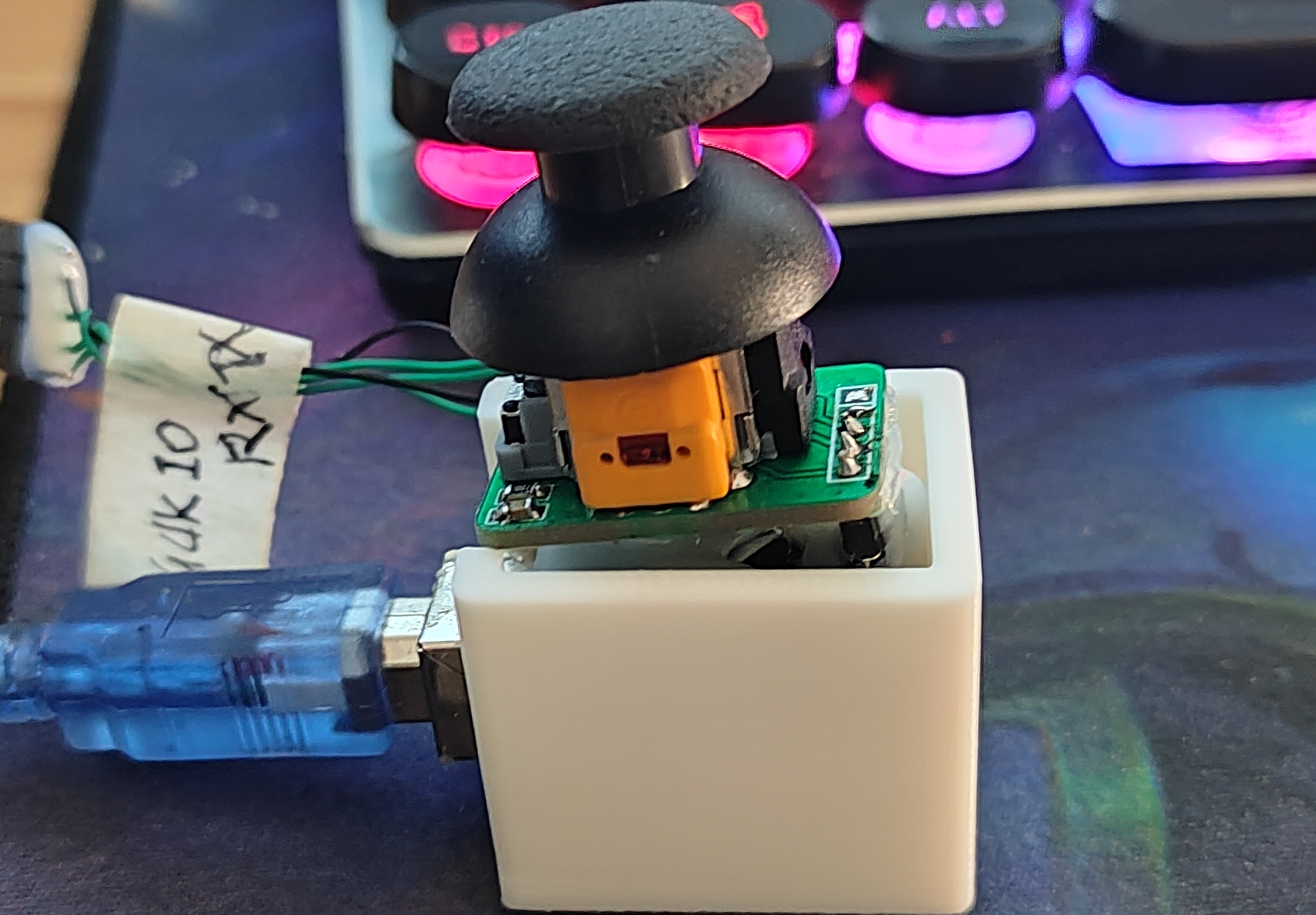
is here: https://www.bilibili.com/video/BV1VM4m1f7KM/?spm_id_from=333.999.0.0 II. Hardware Components : Three stacked boards: Final Version_Plug, Final Version_STM32C8T 6. Final Version - Joystick (Other boards are discarded) Solder the three boards from bottom to top. The main material is a joystick: https://item.taobao.com/item.htm?_u=o2n6g0pabcea&id=745893445759&spm=a1z09.2.0.0.60742e8dyvxAdl&skuId=5317218191530 Note: Jumper wires are needed here: UART + SWD. Connect the solder directly to select the boot mode. Connect all to GND to boot from flash (refer to the schematic for normal boot). This is the MCU. The reset jumper cap can be soldered to horizontal male pins or a toggle switch. This is the jumper cap for enabling the joystick. The LED indicator will light up after the reset is not triggered and the joystick is enabled. III. General Software Framework + Program Source Code: The STM32F103C8T6 is used as the main controller, reading the ADC values of the dual-channel joystick (electromagnetic version will not drift). Then, the on-chip USB-FS is used as a HID keyboard-like device. Based on the ADC segment values, the USB interrupt mode sends ASDW to indicate whether the joystick is pressed or released. The program source code can be directly burned into the STM32 firmware on Gitee (attached). Software Notes: If the upper and lower limits of the joystick voltage you purchased are not 0~3.3V, you need to adjust the main function. Use a multimeter to measure and modify the values of these 6 lines, then compile and burn (you can see that mine is 0~3.23V).


joystick_f103c6t6.axf
PDF_aswd joystick keyboard.zip
Altium_aswd joystick keyboard.zip
PADS_aswd joystick keyboard.zip
BOM_aswd Joystick Keyboard.xlsx
91174
Digital voltmeter and current meter, based on the "LCSC CW32 Development Board".
Digital voltage and current meters based on the "LCSC GeoStar (CW32F030C8T6) Development Board" - JLCSC training camp student assignment.
This voltmeter and ammeter project
is based on the "LCSC CW32F030C8T6 Development Board" digital voltmeter and ammeter, and is a student assignment from the JLCSC Training Camp.
Original example project: LCSC CW32 Digital Voltmeter and Ammeter Expansion Board.
Foreword:
After half a year, I participated in the JLCSC Training Camp again. Half a year ago, I was a complete novice in embedded development. Through the training camp, I gained initial exposure to the embedded development process and understood the general development steps. Half a year has passed, and through sporadic learning in my spare time, I feel I've become a beginner-level enthusiast. I was quite happy to see the news of this training camp opening; finally, I could write a project to practice and consolidate my learning.
This voltmeter and ammeter project seems simpler than the simple digital oscilloscope project I participated in last time, so I made some modifications to the circuit. I envisioned this meter having three functions: voltage measurement, current measurement, and resistance measurement, all using a single set of probes. I wanted it to be as small as possible so that I could hold it in my hand to see the results without turning my head to look at the meter.
Actually, I didn't change much; I mainly added some MOSFETs to control the on/off state, which should have been quite simple... my foot! I was dumbfounded after the first soldering; it was completely unusable. I checked the schematic bit by bit, and discussed it with the group members. We discovered many problems, such as reversed drain-source connections and using an NMOS as the active transistor—these were fatal errors. There were also ridiculous issues like adding a decoder and discovering that multiple MOSFETs couldn't be turned on simultaneously. "Don't add unnecessary things," Occam's words were true.
After the first failed attempt, looking at the limited time left, I had already given up hope and planned to submit it a few days late. But just as delayed justice isn't necessarily justice, what does a late submission matter? In my mind, "completing an assignment" has always been defined as "on time." So I spent two nights redrawing a version, which was indeed a bit messy (and there were a few silkscreen errors). When prototyping, I resolutely chose green. JLCPCB's speed was gratifying; I thought I would receive the board on the deadline, but I didn't expect to receive it a day and a half earlier than I anticipated, when SF Express knocked on the door. So I soldered, modified the code, and debugged in one go, finally managing to get it functioning reasonably well.
Below, I'll introduce this project.
Overall

, the main features include a multimeter with DC voltage, current, and resistance measurement functions. Users can manually select each function, and the measurement range automatically switches. Within the limits of the assignment (using the LCSC CW32 development board), a sandwich structure is used to minimize its size.
A demonstration video
is attached in
the hardware section
. I will compare it with the example project in my description; due to space limitations, I won't go into detail about the original project. Please refer to the link at the beginning of this article. Regarding
the power input

, I'd like to mention that Engineer Li was incredibly detailed, covering everything from LDO selection, why an LDO was used instead of a DC-DC converter, and which capacitor should be placed first (large or small), etc. He explained many very detailed things, which was very helpful for a beginner like me.
Engineer Li mentioned that reverse connection can be prevented using a reverse-parallel diode, which I think is the case, so I made that adjustment. I didn't change the LDO; I think Mr. Li's choice was excellent. Although I didn't buy this particular LDO, I couldn't find a more suitable option for 30V VIN. Also, I initially thought that since I was making a small board, it wouldn't support such a high voltage, but considering how convenient it would be to power the meter using the board during development, 24V is still necessary. Mr. Li also mentioned that the original circuit used a 10k current-limiting resistor for the LED, which is glaring and saves power—it's incredibly thin! However, I think a 10k resistor wouldn't light up my surface-mount LED, so I used a 1.5k resistor.
Regarding

the voltage reference chip, I'm actually quite confused. I feel that the wiring should follow the schematic, and I asked GPT, and it seems that's better, but I don't know if that's true. However, this makes routing difficult, and given the time constraints, I just wanted it to be connected. I don't know if my understanding is correct; the example projects and the two projects I found online also seem to prioritize connectivity over a separate feedback circuit. I hope someone knowledgeable can provide some guidance.
I recall the original circuit for this voltage reference was for calibration, but I didn't have time to do it, and the limited board space prevented me from adding this function. However, I used it to power the resistor sampling circuit, so I kept it. Regarding the
voltage sampling ,

aside from my previous incorrect drain-source drawing, I also drew the NMOS transistor on top, which I initially thought wouldn't have an impact, but testing showed it doesn't work. It seems that if the NMOS is used as the upper transistor, the Rds resistance is close to 0 at the moment of conduction, so the voltage across switch (s) is close to the current (d). Therefore, to maintain the conduction state, Vg must be greater than Vgs(th) + Vs, preventing full conduction.
Here, I used the NMOS as the lower transistor to control the selection of the lower resistor. The software defaults to a large range, automatically switching to a small range if the voltage is below the threshold. As for
current sampling

, this circuit is for learning purposes only; the actual performance is not ideal.
Here I introduced an amplifier circuit, which seems to be specifically designed to amplify the voltage across the sampling resistor. It appears to be just an inverting amplifier circuit with two additional resistors connected to the positive input, but it can be used for high-side sampling. However, I can only use low-side sampling here because all my functions share a single set of probes, and the black probe must be grounded. Additionally, using a regular op-amp results in significant errors when amplifying small voltages; it seems a dedicated current-sensing amplifier is needed in such cases. I originally wanted to add a non-amplified version, but there wasn't enough board space. During soldering, I actually used a 100mΩ amplifier with 10x amplification, which has a much lower error than a 10mΩ amplifier. For
resistor sampling

, I used a simple voltage divider method to measure resistance, aiming for a more accurate voltage. However, it seems the MCU's internal reference voltage cannot be directly used for output? Therefore, I used the 2.5V output from the previous reference voltage. This range is just an example and can be modified as needed. According to my current code, the ADC uses a 1.5V reference voltage, and can only measure up to 150kΩ, which is definitely insufficient for practical use.
Additionally, since this area is ungrounded, I was concerned that placing the NMOS in the middle might not ensure conduction, so I replaced it with a PMOS on the high side. As for
the software
code, I don't really know where to begin; I just rushed through it and there's not much to say.
I'll briefly describe my environment setup.
Because I'm using macOS, I can't use Keil, so I've always developed and learned in the PlatformIO environment (using ARM-GCC), which is how I learned with 51, GD32, STM32, and Arduino. However, since I haven't found a third-party platform package for CW32, I couldn't quickly build a development environment this way.
Later, I set up a CMake environment, called the ARM-GCC compiler, and uploaded it using PyOCD. The relevant configurations are in the code, which is a small feature of this project.
The source code is attached.
Other things
I received from this training camp—component coupons, color silkscreen coupons, panel coupons, and 3D printing coupons—have all been used. It's a pity about the color silkscreen coupon; they sent me ten boards, which was like winning a prize, but unfortunately, the design was wrong. I used both the panel coupon and the 3D printing coupon. The panel file is included in the LCSC EDA project, and the 3D shell file is attached. See the cover for a picture of the actual product.
The conclusion
is both an end and a beginning. It's not the start of the next project, but rather a continuation of efforts to improve this project. This project is far from achieving the results I wanted.
Finally, I sincerely thank JLCPCB and Sinyuan Semiconductor!
volt-ohm-milliammeter_cw32.tar.gz
Demo video.mp4
shell.tar.gz
PDF_Digital Voltage and Current Meter, based on "LCSC CW32 Development Board".zip
Altium Digital Voltage and Current Meter, based on the "LCSC CW32 Development Board".zip
PADS Digital Voltage and Current Meter, based on "LCSC CW32 Development Board".zip
BOM_Digital Voltage and Current Meter, based on "LCSC CW32 Development Board".xlsx
91175
CW32F030C8T6 Voltage and Ammeter_OLED__Network Clock
This project is a voltage and current meter developed based on the LCSC CW32 Diwenxing development board. It can be used for basic everyday voltage and current measurements, with minimal difference in accuracy. For precise measurements, please use a multimeter. This project is only intended for understanding the principles of voltage and current meters.
Video Link:
[Bilibili Video - Function Demonstration and Introduction] https://www.bilibili.com/video/BV1iSWVenErq/?vd_source=dcec384099758377125cc78a52ec1015
Project Introduction:
This project is a voltage and current meter developed based on the LCSC CW32 GeoStar development board. It can perform basic daily voltage and current measurements. The accuracy is similar; for precise measurements, please use a multimeter. This project is only for understanding the principles of voltage and current meters. In addition to the main functions, the board is designed with SPI... The OLED interface is used for displaying voltage and current values. It also features a CH340 serial port output for data transmission and reception. We use the MODBUS communication protocol. Originally, the design involved the host computer sending a request command for the voltage value. However, due to damage to the RX port of the LCSC development board, we adopted an active transmission method, with the output option set via a menu. The main reason for this was the lack of a virtual serial port function on the onboard Type-C, requiring an external USB-TTL connection, which is cumbersome. Additionally, the onboard ESP01S module interface can be used for IoT development, similar to MQTT. Here, we use it as a network clock to request network time data from an API. Due to time constraints, network weather functionality has not yet been implemented.
Project Functionality
: This design is a voltage and current meter based on the LCSC development board - LCSC:
1. It has four buttons: Confirm, Previous, Next, and Return, used for menu operation and function settings.
2. The onboard Type-C-CH340 solves the problem of the LCSC requiring a USB-TTL module, enabling data transmission and reception. Here, it is used to upload voltage and current data to a PC host computer for observing voltage and current stability, trend changes, and repeatability accuracy.
3. Onboard 7-pin SPI OLED interface, also serving as a hardware IIC OLED, for SPI/IIC OLED learning.
4. Onboard ESP01S module interface, for wireless communication learning, IoT learning such as MQTT, network clock, weather clock, etc.
5. Onboard DC socket, input voltage is stepped down to 5V to power the system via a step-down chip.
6. Onboard voltage and current test terminal interface for voltage and current testing.
Materials Purchase:
1. LCSC development board: Diwenxing/Dikuoxing
2. ESP01-S WIFI module, recommended to purchase with the socket for easy serial port debugging
3. 0.96-inch SPI OLED
4. Buttons: Purchase side-mounted ones that extend beyond the casing.
Project Parameters:
1. This design uses a 0.96-inch 7-pin SPI... 1. OLED for voltage and current display, menu display, and clock display
. 2. This design uses the ESP01-S module for network clock acquisition, and can also connect to Alibaba Cloud for data upload and command issuance, enabling IoT development.
3. This design uses the CH340 chip to solve the problem of the lack of a virtual serial port on the satellite.
Principle Analysis (Hardware Description)
: Here you can fill in the design principle of the project, breaking down and analyzing the design principle. Example:
This project consists of the following parts: power supply section, voltage sampling and calibration section, current sampling and calibration section, OLED section, ESP01S module section, USB-Type C section, button section, and LED expansion section. The expansion pin section of this project mainly uses two voltage acquisition circuits to divide different voltages to ensure that the voltage sampled by the input ADC is within a safe voltage range, with a maximum measurable voltage of 30V. The voltage measurement range can be expanded by changing different voltage divider resistors and internal reference voltages. The acquired voltage is output via serial port using the MODBUS communication protocol, which is more suitable for industrial environments. The OLED displays the corresponding voltage and current values. When not using a voltmeter or ammeter, the ESP01-S module is used to connect to the network and request network time. This board can be used as a small network clock, updating and calibrating every 5 minutes.


The display issue is related to the photo capture; the OLED is refreshed
. 1. Power supply circuit:
DC power can be used here, with an input range of 0-30V. The input voltage is reduced to 5V by the SE8550HF circuit. Alternatively, a TYPE-C-16P interface can be used as the power supply interface. The corresponding USB data pins are connected to the CH340 chip, and then to PA9 and PA10 for direct USB serial communication without the need for an external serial converter module. It should be noted that 5.1K pull-down resistors are added to the CC1 and CC2 pins to facilitate identification and configuration by different host devices. Also, since 5V power is used here, according to the datasheet, pin 3 of the CH340E should be connected to 100nF and then grounded.
Here are some details: PA9 and PA10 are used here for compatibility with STM32F103C8T6.


2. Voltage sampling and calibration:
The measured voltage is divided and input to ADC_IN8 and ADC_IN9 respectively. Shorting H7 allows the system voltage to be used as the measured voltage for testing. The input voltage can be adjusted by potentiometer R14. A diode 1N4148W is connected to protect the circuit.


3. Current sampling and calibration:
The current sampling circuit inputs to ADC_IN7. Without connecting R6-100 milliohm resistor, H7 can be shorted to use voltage to simulate current.


4. OLED section
: The pins here use SPI. A detail here is that the SDA pin can be shorted by PB14 or PB15, mainly for hardware IIC when using IIC OLED.


5. ESP01S module section
: The TX and RX pins of the ESP01S module are connected to PA2 and PA3.

6. Button section: The
button section is relatively simple and does not have pull-up pins. Note that the GPIO needs to be configured as a pull-up input.

7. LED expansion section
: The LED expansion circuit can connect to any other I/O.

8. Extended pin section
: Bring out all pins for easy use and debugging.

9. Schematic circuit design:
Here we can see that when I designed the schematic, I intentionally compared the Diwenxing and Dikuoxing boards, so that this board can be used as a development board in addition to completing the design of voltage and current meters. I also checked and the board is compatible with GD32E230C8T6. I haven't looked at other boards yet. When designing, I only combined the Diwenxing and Dikuoxing
software code
programs. For details, please refer to the attachment.
1. ADC sampling section
(1) Collect 4 channels, including the internal reference voltage AI17

(2) The ADC adopts the external trigger mode, and the timer triggers sampling once every 1ms.

(3) Each time it is sampled, the data is pushed into the array. After the data is reached, the array value is averaged and then converted into the corresponding voltage and current value.

(4) In terms of output, when the 3V channel sampling is less than 4095, the 3V channel value is output as the sampling voltage. If it exceeds 4095, it will be converted to the 30V voltage divider channel output.

2. Menu porting:
Add response header file and initialize the function in the lower box.

3. Add the function OLED_UIProc() to the main program;

4. This function automatically connects to WIFI upon power-up. The WIFI name and password in the header file need to be modified.


5. The button part needs to be initialized as pull-up input. An external trigger is used here, detecting button presses in the interrupt and placing the key value into a queue.


6. In the main loop, check the following flags and set them accordingly.

7. Connect to Alibaba Cloud. Here, data can be uploaded to the Alibaba Cloud server, or commands can be sent from Alibaba Cloud for control. Here, commands are sent to turn on the LED
. The triplet needs to be modified. Related tutorials can be found on CSDN.


Note
: When connecting the OLED, the SDA-PB15 pin of H2 needs to be shorted; otherwise, it will not light up.

Soldering:
It is recommended to solder CH340E first, then solder the C-pin. Use solder paste sparingly to avoid solder bridging. If possible, use a hot air gun with a low airflow. The
assembly process
involves first inserting the buttons, then

snapping on the cover

and screwing it in. The casing design is quite sophisticated; pillars are used to secure

it. ( Images
of the PCB and menu interface are

included .) The casing design features : 1. Side-mounted buttons for easier access ; 2. Power and communication ports ; 3. Rear panel with wireless module antenna output and voltage/current interface terminals; 4. Right-side output for download port wiring; 5. 1.6mm spacing between screw pillars, which is ideal for a 1.6mm board. The panel uses a custom-developed host computer that uses the MODBUS protocol to monitor current trends and adjustments, assess stability, and test repeatability. Attachments include: power supply measurement values compared with a multimeter ; J-Link power supply comparison program source code, etc.


CW32F030C8T6_Eiker_5441715A.rar
1.mp4
2.mp4
3.mp4
4.mp4
5.mp4
6.mp4
7.mp4
8.mp4
PCB.zip
Color PCB.zip
panel.epanm
Host computer.rar
PDF_CW32F030C8T6 Voltage and Current Meter_OLED__Network Clock.zip
Altium_CW32F030C8T6 Voltage and Current Meter_OLED__Network Clock.zip
PADS_CW32F030C8T6 Voltage and Current Meter_OLED__Network Clock.zip
BOM_CW32F030C8T6 Voltage and Ammeter_OLED__Network Clock.xlsx
91176
ESP32-based desktop dashboard
It uses the LCSC ESP32S3R8N8 development board. It can display various computer performance indicators in real time, and also features temperature and humidity detection, low-power sleep mode, automatic brightness, and OTA upgrades. The menu is based on a secondary development of WouoUI, offering a smooth and fluid experience.
This is a desktop dashboard based on ESP32
. The project is available at:
https://github.com/vrxiaojie/ESP32-desktop-dashboard
and https://oshwhub.com/vrxiaojie/esp32-based-desktop-dashboard . It uses the
LCSC
ESP32S3R8N8 development board.
It can display various computer performance indicators in real time, and also features temperature and humidity detection, low-power sleep mode, automatic brightness, and OTA upgrades. The menu is based on WouoUI and is smooth and fluid.
2. Hardware
The hardware components required are as follows
: | Name | Quantity |
|:---:|:---:|
|LCSC ESP32-S3R8N8 Development Board|1|
| 0.96-inch OLED Screen 128*64 Resolution|1|
| BH1750 Module|1|
| SHT40 Module (Optional)|1|
3. Software
3.1 PC-side Python Program
import json
import psutil
import GPUtil
import random
import time
import paho.mqtt.client as mqtt_client
def PC_Info():
msg = dict()
msg["CPU_usage"] = str(psutil.cpu_percent(interval=1))
msg["CPU_Frequency"] = str(round(psutil.cpu_freq().current / 1000.0, 1))
msg["RAM_usage"] = str(psutil.virtual_memory().percent)
gpu = GPUtil.getGPUs()
for gpu in gpu:
msg["GPU_temp"] = str(gpu.temperature)
msg["GPU_memory"] = str(gpu.memoryUsed)
msg = json.dumps(msg, ensure_ascii=False)
# print(msg)
return msg
# Configure MQTT server
host = '192.168.50.111'
port = 1883
# Configure MQTT client
topic = "/python/esp32_mqtt" # Create topic, can be customized
client_id = f'python-mqtt-{random.randint(0, 100)}'
username = 'python'
password = '123456'
def publish(client, msg):
result = client.publish(topic, msg)
def connect_mqtt():
def on_connect(client, userdata, flags, rc):
if rc == 0:
print("Connected to MQTT Broker!")
else:
print("Failed to connect, return code %d
", rc)
client = mqtt_client.Client(client_id)
client.on_connect = on_connect
client.username_pw_set(username, password)
client.connect(host=host, port=port)
return client
def run():
client = connect_mqtt()
client.loop_start()
while True:
msg = str(PC_Info())
publish(client, msg)
time.sleep(0.5)
if __name__ == '__main__':
run()
3.2 There are currently two methods to obtain firmware for flashing
: 1.
Obtain the .bin file from the GitHub Release folder
: Clone the GitHub repository and manually configure the PlatformIO environment. 2. Compile and
flash:
Connect the development board to the computer using a Type-C cable. Use the flashing tool provided by Espressif (https://www.espressif.com.cn/zh-hans/support/download/other-tools)
. Download the firmware to the device using PlatformIO
(only for successful flashing once). Select OTA upgrade from the menu. Connect the computer to the device's Wi-Fi, open a webpage (192.168.4.1), and select the firmware downloaded from the Release folder.bin file upgrade
4 3D shell
The 3D shell was drawn using LCSC EDA. Please open and view the open-source link with an editor.
Nylon material is recommended; it's a bit pricey, but the appearance and texture are excellent.
5. Appearance Showcase

6. Acknowledgements:
UI based on WouoUI, original author's repository: https://github.com/RQNG/WouoUI
ESP32 Desktop Dashboard.mp4
PDF_ESP32-based Desktop Dashboard.zip
Altium_ESP32-based Desktop Dashboard.zip
PADS_ESP32-based Desktop Dashboard.zip
BOM_ESP32-based Desktop Dashboard.xlsx
91177
GL3231 Overclocking SD/TF Card Reader
A dual-card reader that supports the USH-I overclocking card, supporting SD cards (with read/write protection) and TF cards, with a theoretical maximum read speed of 160MB/s and an actual read speed of 180MB/s.
Note: Commercial use and mass production/sale are prohibited without permission!!!
-------------------------------------------------------- Divider --------------------------------------------------
Note: Do not remake if you do not have the firmware!!! Testing has shown that this controller, without firmware, can only read and write to a single card and cannot use DDR200 speed mode (160mb/s overclocking mode).
For those who want to experience it in advance, I have listed the GL3231 chip and Flash chip (with firmware already burned) on Xianyu. Click the link below to view.
Xianyu link: https://m.tb.cn/h.gN3Al7G?tk=lYe13fUar8NHU9046
"I have posted 【GL3231 chip overclocking card reader controller】 on Xianyu"
-------------------------------------------------------- Divider --------------------------------------------------
Previously, I made a GL3224 card reader, which used a USH-I overclocking card, but could not fully utilize the card's performance.
This is the GL3224 dual-card dual-reader: https://oshwhub.com/engineer_jiang/gl3224-du-ka-qi-_-shuang-ka-shuang-du
I've modified the GL3224 to support G2 board USB drives, EMCP221/EMMC153 + TF card dual reading: https://oshwhub.com/engineer_jiang/ji-yu-gl3224-qfn48-zhu-kong-emmc-du-xie-fang-an
This GL3231 card reader has been tested and the results are very good. It steadily manages the heat generated by the Kingston Blue Bar, but the downside is that the 4K speed isn't quite up to par.
-------------------------------------------------------- Divider --------------------------------------------------
Main Controller GL3231:
The GL3231 is a USB 3.1 Gen1 to dual SD 3.0 LUN Memory Card Reader controller. The GL3231 supports various SD memory cards, including Secure Digital™, SDHC, miniSD and microSD (T-Flash), MultiMediaCard™, RS-MMC, MMCmicro, and MMCmobile. It also supports high-density memory cards such as SDXC, high-speed memory cards, and SD 3.0 UHS-I (maximum capacity 2TB). The GL3231 also supports SANDISK EXTREME 160mb/s microSD UHS-I cards.
Commercially available products using the same controller include SanDisk Pro-Reader, Lexar RW310U, and RW310X.
The image below shows the speed test results of the SanDisk Pro-Reader card reader; the following text shows the test results of a custom-made card reader.


The custom-made card reader

features a modified side panel and a hidden SD/TF card design, resembling an Msata hard drive enclosure.


The PCB is shown in the image; the Type-C female connector is front-mounted and rear-mounted for a more secure fit, and all card slots are spring-loaded.
Read/Write Speed Test:
Test Conditions: Kingston Blue Stripe SDCG3 512G TF card, exFAT format; thermal paste was applied to both the controller chip and the TF card slot, allowing for close contact with the aluminum alloy casing; ambient temperature around 25℃, no active cooling.

1. AS SSD test

2. CrystalDiskMark test

Evaluation: Performed normally, as these are peak speeds.
3. ATTO test

4. urwtest full disk read/write test

Evaluation: Notably, there was no heat or speed reduction during full disk read/write, although the card reader casing became warm.
5. HD Tune 1G read/write test

Evaluation: The 1G write speed appears somewhat volatile; only one test was performed, so this is just for reference.
6. HD Tune 40G read/write test

Evaluation: The 40G read/write speed appears very stable with minimal fluctuations.
PDF_GL3231 Overclocking SD-TF Card Reader.zip
Altium_GL3231 Overclocking SD_TF Card Reader.zip
PADS_GL3231 Overclocking SD/TF Card Reader.zip
91179
Digital voltmeter and ammeter
Digital voltmeter and ammeter
This digital voltmeter and ammeter is based on the LCSC Diwenxing CW32F030C8T6 development board.
This project originates from the LCSC development board voltmeter and ammeter training camp, with some simplifications in functionality and design.
I. Functionality
: Only two functions are retained:
1. Voltage measurement (0-30V)
2. Current measurement (0-3A).
The measurement method borrows from a multimeter, using positive and negative probes connected across the circuit being measured.
II. Schematic Design:
To accelerate development, this project uses the LCSC Diwenxing development board. Therefore, the core task becomes how to use the ADC pins provided by the MCU to measure voltage. The main design ideas are as follows:
1. Since the development board already includes a complete LDO circuit, this part of the circuit is omitted in the schematic. The advantage is that it greatly reduces the number of components in the BOM. The inconvenience is that the development board must be powered during measurement. Since the core requirement of this project is voltage and current measurement, rather than the design of peripheral circuits, this was chosen to be omitted.
2. The external interface design also follows a minimalist principle, retaining only two probe sockets and a slide switch. This design is based on the desire to create a simple tool, and simple tools typically have a concise design for ease of use. The
entire schematic includes the following parts:
1. Development board interface: Connects to the LCSC/Diwenxing development board via two 20-pin female connectors. The voltage required for the sampling circuit clamping is obtained from the development board's 3.3V port.
2. Voltage and current sampling section: This section uses the same components as the training camp, aiming to examine the sampling accuracy of the CW32F030 MCU's native ADC. Voltage and current are switched via the SW1 slide switch. This saves a digital display.

Voltage measurement is performed using a resistor divider, with an appropriate voltage division ratio designed according to the measurement range. Furthermore, a diode (1N4148) clamping mechanism controls the voltage entering the MCU pins within a safe range.
In selecting the two voltage measurement values (program-controlled), when the measured result is greater than 3V, the value of the ADC_IN1 pin is selected. If it is less than or equal to 3V, the result of the ADC_IN2 pin is automatically selected for display to improve measurement accuracy.
This design uses the 3.3V clamping voltage provided by the development board. The voltage drop of the 1N4148 is typically 1V, so theoretically, the current entering the MCU pin should be below 4.3V. Referring to the CW32F030 datasheet, the maximum voltage of the IO port is Vdd + 0.3V, approximately 6.3V. (If you want to replicate and perform high-voltage measurements, ensure that the highest voltage at the ADC_IN2 point does not exceed 6V, otherwise it may damage the MCU pin).

The current sampling resistor is a 100mΩ, 1W package, consistent with the training camp specifications. Based on the actual current measurement results, this part has considerable room for optimization. For example, a more professional sampling resistor could be selected, or an amplifier circuit could be used.
3. LED digital tube section: used to display the measured voltage or current values. The MCU's GPIO ports are directly connected to the digital tube. Different numbers are displayed by controlling the high and low levels of the GPIO ports.
III. PCB Design:
Due to the relatively simple circuit, PCB routing is not difficult. It is important to note that the current sampling circuit needs to consider the throughput of 3A current. Additionally, suitable surface-mount components can be selected for the sampling circuit to further improve the aesthetics of the layout.
IV. Code:
The user code logic is as follows:
1. Initialize the development board clock (board.c).
2. Configure the LED digital tube (display.c).
3. Configure the acquisition IO ports (measure.c).
4. Configure the timer and complete the interrupt handling logic (interrupts.c): process the data acquired from the three acquisition ports every 1ms. When switching to the voltage measurement circuit, ADC_IN1 and ADC_IN2 ports have values. If the voltage of ADC_IN1 is greater than 3, that value is used for display. Otherwise, the data from ADC_IN2 is used. When switching to the current measurement circuit, theoretically, the readings of ADC_IN1 and ADC_IN2 should be 0. At this point, it is determined that a circuit measurement is being performed, and the data from the ADC_IN3 port is used for display.
V. Materials
All components in this project are from LCSC, except for the following:
1. Multimeter probes
2. Multimeter probe socket
VI. Assembly Instructions
1. The purchased multimeter probe socket is relatively tall. To minimize the overall height of the project's casing (currently designed to be 25mm), the screws at the bottom of the socket need to be shortened (I used a hacksaw). If you want to replicate it, you can look for a shorter socket.
2. Connect the leads from the probe socket to the CN1 pin header via connectors.
3. Secure the upper casing with four M2 screws. If you want to replicate it, please consider the PCB board fixing (you can add stiffeners to the four corners of the lower casing and use them in conjunction with the four studs on the upper casing to press the PCB firmly). Additionally, you need to pre-tap the screws on the upper casing or pre-embed nuts.
VoltageAmmeter-MDK code project.zip
Actual test.mp4
3D Shell.zip
PDF_Digital Voltage and Current Meter.zip
Altium Digital Voltage and Current Meter.zip
PADS Digital Voltage and Current Meter.zip
BOM_Digital Voltage and Current Meter.xlsx
91180
CW32F030C8T6 Voltage and Current Meter
LCSC GeoStar CW32 Digital Voltage and Current Meter Expansion Board
The problem requires
referencing
the official documentation for the LCSC Diwenxing-CW32F030C8T6 voltage and current meter
(https://wiki.lckfb.com/zh-hans/
). The problem analysis
involves voltage acquisition using an ADC (Analog-to-Digital Converter) with a 12-bit ADC and a reference voltage of -2.5V to reduce the voltage range from 0 to 30V. The resulting analog signal is then converted to the actual voltage value using code.
For current acquisition, a high-side sampling resistor is used. The voltage drop across the sampling resistor is amplified to the mV level by an operational amplifier, allowing the ADC to acquire the analog signal, which is then converted to the actual current value.
Schematic Design Description

I. MCU Selection This project uses the LCSC CW32F030C8Tx development board (core board) as the main controller.
The CW32's key advantages in this project include
: Wide operating temperature range: -40 to 105℃;
Wide operating voltage: 1.65V~5.5V;
Strong anti-interference: HBM ESD 8KV; All ESD reliability reaches the highest international standard level (STM32 ESD 2KV); A key feature of
this project is its superior ADC: 12-bit high-speed ADC achieving ±1.0LSB INL 11.3ENOB; Multiple Vref reference voltages (internal 1.5V, 2.5V reference voltage can be selected) or an external reference voltage can be selected. This allows for measurements with varying accuracy at different voltages;
Stable and reliable eFLASH technology.
II. Voltage Sampling Circuit:
This project designs a two-group voltage divider with precision low-temperature drift resistors of 200K+10K/100K+10K,
with voltage division ratios of 20:1 (ADC_IN11) and 10:1 (ADC_IN6). This proportionally reduces the input voltage, which is then measured by the ADC to obtain a digital value, which is then converted into a voltage value. The use of low-temperature drift and high precision ensures more accurate measurement values.

III. Current Sampling Circuit :
This project uses a 5mR sampling resistor for current detection. When current flows through the sampling resistor, a voltage value is generated. This voltage value is very small, so it is amplified by an operational amplifier, and then sampled by the ADC to obtain the specific value.

IV. Expansion Circuit:
a. A monochrome OLED is used for data display. The purpose of using a plug-in screen is to save learning costs and make the OLED expandable.
b. A passive buzzer is used for indication. Since it's a passive buzzer, it requires a specific frequency to drive, thus utilizing the CW32's PWM output.

c. It addresses the inconvenience of not having a power source when traveling, allowing for switching between lithium battery operation and power supply via the development board's TYPC. It also features lithium battery level detection, using a buzzer to indicate low voltage. The charging circuit uses the development board's built-in TYPC for simultaneous charging during operation. The TP4O56 charging chip used is a classic, inexpensive, and reliable chip, offering charging detection and completion indicators for added convenience.


d. LEDs are the most prominent indicator signals. My circuit has three LEDs: a green LED displays the normal 3.3V power supply; a red LED indicates low battery and charging; and a blue LED indicates a fully charged battery.
PCB Design Notes
: 1. When designing the board, first consider the required shape, size, and intended use.
II. Due to the need for excessively high voltage and current, copper reinforcement should be used as much as possible, and signal lines should not be bent too much.


Software Description:
ADC (Analog-to-Digital Converter) is an indispensable key component in electronic systems. It converts continuous analog signals into digital signals, enabling digital processing and analysis. ADCs play an important role in signal conversion, measurement and data acquisition, control system input, and communication and signal processing. Their widespread application promotes the intelligent and precise control of electronic equipment in various industries and is one of the key factors driving modern technological progress.
Therefore, to achieve simultaneous voltage and current sampling, an ADC sequence channel is used for acquisition. The CW32 has 4 sequence channels. Both voltage and current are averaged to obtain stable values.

I. Voltage Sampling


II. Current Sampling


Physical Demonstration

Notes:
Simultaneous voltage and current measurement is possible without interference. A 3.3V power supply is used during testing, and three power supply methods are available: 1. Type PC. 2. Lithium battery power. 3. 3.3V wired power.
30V voltage.mp4
Low voltage.mp4
Current.mp4
CW32 Voltage and Current Meter.rar
PDF_CW32F030C8T6 Voltage and Current Meter.zip
Altium_CW32F030C8T6 voltage and current meter.zip
PADS_CW32F030C8T6 Voltage and Current Meter.zip
BOM_CW32F030C8T6 Voltage and Current Meter.xlsx
91181
0-10V/0-20mA signal generator based on CW32ADC
A voltage and current (0-10V/0-20mA) and pulse AB phase generator based on the CW32ADC microcontroller, and accurately monitors its voltage and current output.
Design Background:
In the field of industrial automation, 4-20mA current signals, 0-10V voltage signals, and AB phase pulse signals with phase difference are widely used. In conjunction with the LCSC CW32 voltage and current meter training camp held in July-August 2024, this project utilizes the LCSC CW32F030C8T6 development board to implement these functions and accurately measure and monitor the output voltage and current.
Project Features:
The LCSC CW32F030C8T6 development board features 12 12-bit ADC input points and abundant hardware and software documentation. The official website also provides a large number of programs for porting.
1. The CW32 ADC is used to achieve accurate voltage and current detection .
2. The 0-10V/0-20mA voltage and current generator is implemented using an operational amplifier.
3. Voltage and current control can be achieved using a CW32F030C8T6 microcontroller in a numerical control manner. The microcontroller generates an adjustable PWM signal, which is converted into a voltage signal by a low-pass filter and then amplified by an LM358 to increase its load-carrying capacity.
4. The encoder is used to control the addition and subtraction of current and voltage signals, and also to generate pulse output signals.
The overall design scheme block diagram
is divided into three main modules and 12 sub-modules.

The hardware design description
includes three schematic diagrams: the main control display circuit, the charging circuit, and the voltage and current generator.


Instructions: 1. Voltage measurement sampling is performed in the 0-10V voltage measurement sampling block diagram in Schematic 1, and current sampling is performed in the 0-20mA current measurement sampling block diagram in Schematic 1. Since the output current and voltage share a common ground, current sampling can only be performed at two points, I_SMP1 and I_SMP2. Then, according to the formula: Current = Difference between two voltages / Sampling resistor, the battery voltage measurement is performed in the battery voltage block diagram. This circuit has a total of 4 analog input ADCs, which are connected to ADC_IN8, ADC_IN9, ADC_IN11, and ADC_IN12 respectively.
2. The microcontroller uses the LCSC CW32F030C8T6 development board, which uses a dual-row 40-pin IC socket. The development board can be directly plugged into it, which is very convenient. The LED digital tube display circuit uses two 0.28-inch 4-digit common cathode digital tubes. The same model is used in the design. When purchasing specific components, you can buy one red and one white for a more aesthetically pleasing appearance when lit. There are many tutorials online for the specific hardware circuit principle, which will not be elaborated here.
3. Power supply uses a dual-power supply of a 3.7V lithium battery and a 5V Type-C port. Charging is performed simultaneously with the 5V Type-C port power supply. A TP4054 is used for charging. An ME6231 LDO provides a stable 3.3V power supply to the CW32 development board. The 3.3V on the motherboard needs to be connected to the 3.3V on the CW32 development board. A 12V boost circuit FP6291LR provides power to the 0-10V, 0-20mA signal generator. An LM358DR dual op-amp is used. Considering the load capacity of the current source, the 12V power supply can be boosted to 24V later to match industrial applications.
4. Encoder input is used to control the microcontroller's PWM pulse width adjustment. Different PWM signals with different pulse widths are generated based on the number of rotations. R49 and C42 are first-order low-pass filters that convert the PWM signal into a voltage signal. This signal is then amplified by an operational amplifier to improve the load capacity, and finally amplified again by another operational amplifier to convert the voltage into current, generating a 0-20mA current signal.
5. Pulse Output: AB phase pulses generated during manual encoder rotation are synchronously output to the extended output port for use with industrial stepper servo motor drivers.
PCB Design Notes:
The PCB is generated directly from the schematic. Three function buttons are placed on the top. Voltage and current outputs use 2P ports, and the pulse output 4P port is also placed on the top. The LED digital tube is placed in the upper-middle part of the front panel. Next is the encoder, placed on the center line. The voltage generator circuit is to the right of the encoder, and the current generator circuit is to the left. The CW32 development board is placed in the lower middle section, followed by the charging port, power converter, and 3.3V circuit. The layout follows LCSC EDA's guidelines; numerous online videos explain the specific layout and routing methods.

The 3D shell is a standard top and bottom cover structure. The top button design includes three button caps and a switch handle.


During 3D shell simulation, it was found that the LED digital tube sank too low. When soldering the circuit board, the digital tube pins should not be cut off; they should be soldered higher.
Because my development board is plugged into an IC socket, the entire circuit board is quite thick. The LED digital tube needs to be taller than the development board, so even without cutting the pins, it's not tall enough. Therefore, I added mounting brackets on top to raise the height of the LED digital tube.


The panel printing was also designed according to LCSC EDA's panel design tutorial.

Software Description:
The so-called software program refers to learning how to port programs, which can save a lot of trouble. Specifically, the software uses Keil uVision5, porting and improving the voltage and current meter program from the LCSC CW32 voltage and current meter training camp. Details can be downloaded from the attached program; this is just an explanation.
ADC.C is configured with four channels for analog-to-digital conversion:
PB01_ANALOG_ENABLE(); // Enable analog pin IN9 0-10V
PB00_ANALOG_ENABLE(); // Enable analog pin IN8 Ui1 Current sampling point 1
PB10_ANALOG_ENABLE(); // Enable analog pin IN11 Battery voltage
PB11_ANALOG_ENABLE(); // Enable analog pin IN12 Ui2
Current sampling point The sampled data is stored in:
uint16_t Volt_Buffer[ADC_SAMPLE_SIZE];//Voltage sampling
uint16_t I_Samp1_Buffer[ADC_SAMPLE_SIZE];//Current sampling 1
uint16_t I_Samp2_Buffer[ADC_SAMPLE_SIZE]; // Current sampling 2
uint16_t BatVolt_Buffer[ADC_SAMPLE_SIZE]; // Battery sampling
Then, the mean filtering program is called in the main program to obtain the values of 4 analog signals.
Seg_dis.c is the digital tube display program,
ec11.C is the rotary encoder program, which configures CW_BTIM2 as the timer for the rotary encoder's timing scan.
void GTIM1_PWM_Init(void) and void PWM(void) are used in the main program main.c to generate PWM


 京公网安备 11010802033920号

 VN050H(011Y)


